System for fabricating liquid crystal display and method of fabricating liquid crystal display using the same

a liquid crystal display and liquid crystal technology, applied in non-linear optics, instruments, optics, etc., can solve the problems of reducing productivity, taking too much time for liquid crystal injection, and failing to fill the inside of the panel completely, so as to reduce process time and improve productivity.

Inactive Publication Date: 2005-11-10
LG DISPLAY CO LTD
View PDF44 Cites 39 Cited by
  • Summary
  • Abstract
  • Description
  • Claims
  • Application Information

AI Technical Summary

Benefits of technology

[0031] An object of the present invention is to provide a system for fabricating a liquid crystal display using liquid crystal dropping and method of fabricating a liquid crystal display using the same enabling to reduce a process time and improve a productivity.

Problems solved by technology

In spite of various technical developments to perform a role as an image display in various fields, an effort to improve image quality of LCD inevitably becomes contrary to the above characteristics and advantages in some aspects.
First of all, it takes too much time for liquid crystal injection to reduce productivity since the liquid crystals are injected therein by maintaining the vacuum state between the two substrates.
Secondly, in fabricating a large-sized liquid crystal display, the liquid crystal injection method fails to fill completely an inside of the panel with liquid crystals so as to bring about failure.
Finally, the process becomes so complicated to waste process time as well as requires a plurality of liquid crystal injection instruments to fail to save a space.
Hence, there is unbalance between processes for the first and second substrates, thereby failing to operate a product line effectively.
Third, because the sealant is coated on the first substrate as well as the liquid crystals are dropped on the first substrate, it is unable to clean the substrate coated with the sealant in a cleaning equipment(USC).
Hence, the sealant bonding the substrates to each other is unable to be cleaned to remove particles therefrom, thereby bringing about failure caused by the particles in the sealant on bonding.
Fifth, it is difficult to drop a precise amount of the liquid crystals on dropping, excessive charge of the liquid crystals makes the liquid crystals run down, and insufficient charge of the liquid crystals varies a cell gap so as to affect an image quality.

Method used


Image

  • System for fabricating liquid crystal display and method of fabricating liquid crystal display using the same
  • System for fabricating liquid crystal display and method of fabricating liquid crystal display using the same
  • System for fabricating liquid crystal display and method of fabricating liquid crystal display using the same

Examples


first embodiment

[0141] First Embodiment

[0142]FIG. 5 illustrates a layout of an LCD for explaining a column spacer according to a first embodiment of the present invention.

[0143] Referring to FIG. 5, a liquid crystal display according to a first embodiment of the present invention includes first and second substrates 10 and 20, and a UV hardening sealant 30 is formed at a periphery area between the substrates 10 and 20.

[0144] And, a column spacer(not shown in FIG. 5) is formed in a pixel area(a line ‘A’ is a virtual line to distinguish the pixel area). And, a dummy column spacer 28 for controlling a liquid crystal flow is formed inside the UV hardening sealant 30 in a dummy area of the pixel area periphery.

[0145] And, a liquid crystal layer(not shown in the drawing) is formed between the substrates 10 and 20.

[0146] In this case, the column spacer 27 is formed to have the same level of a cell gap between the first and second substrates 10 and 20 so as to maintain the cell gap.

[0147] Moreover, th...

second embodiment

[0164] Second Embodiment

[0165]FIG. 7 illustrates a layout of an LCD for explaining a column spacer according to a second embodiment of the present invention.

[0166] Referring to FIG. 7, a second embodiment of the present invention relates to a liquid crystal display including a dummy column spacer 28 so that a plurality of openings 29 are formed at each of the corner areas of a substrate.

[0167] A plurality of the openings 29 are formed so that liquid crystals enable to move to the corner areas of the substrate to prevent insufficient charge of the liquid crystals.

[0168] The openings 29 are formed at one of the corner areas at least so as to be formed consecutively or discontinuously.

[0169] And, the rest elements of the liquid crystal display are the same of the liquid crystal display according to the first embodiment of the present invention.

third embodiment

[0170] Third Embodiment

[0171]FIG. 8 illustrates a layout of an LCD for explaining a column spacer according to a third embodiment of the present invention.

[0172] Referring to FIG. 8, in a third embodiment of the present invention, a column spacer(not shown in FIG. 8) is formed in a pixel area(a line ‘A’ indicates a virtual line to distinguish the pixel area), and first and second dummy column spacers 28a and 28b are formed inside a UV hardening sealant 30 in a dummy area of a periphery of the pixel area so as to control a flow of liquid crystals. The first and second dummy column spacers 28a and 28b are formed as tall as the column spacer. And, an opening 29 is formed at a corner area at least.

[0173] Namely, a dotted-line type second dummy column spacer 28b is formed in the dummy area inside the first dummy column spacer 28a so as to assist the liquid crystal flow control.

[0174] Thus, the dotted-line type second dummy column spacer 28b is formed additionally inside the first dumm...


PUM


Abstract

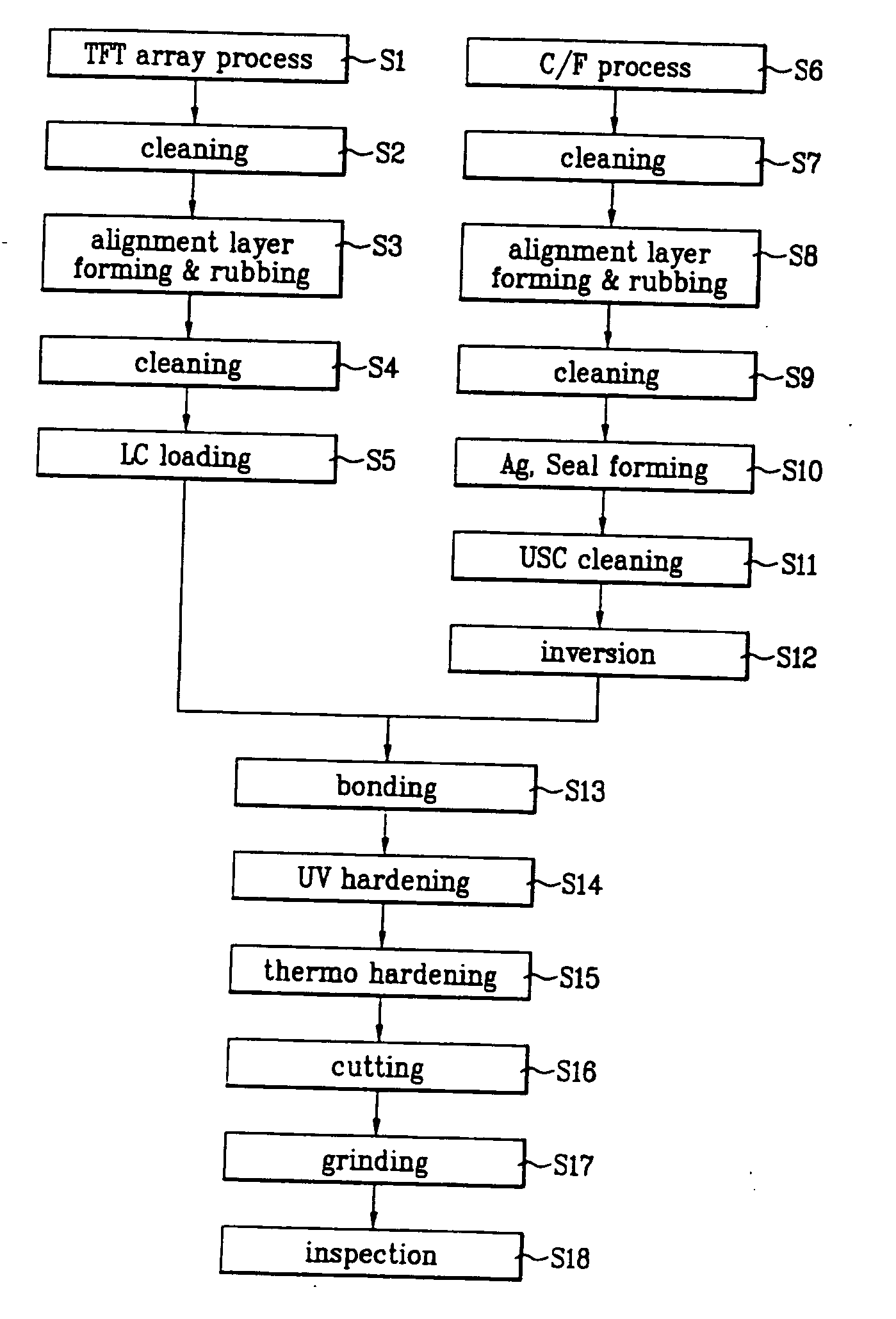
Disclosed is a system for fabricating a liquid crystal display using liquid crystal dropping and a method of fabricating a liquid crystal display using the same. The present invention includes a liquid crystal forming line dropping liquid crystals on the first substrate, a sealant forming line forming the sealant on the second substrate, and a bonding and hardening line bonding the two substrates to each other and hardening the sealant, printing a sealant, bonding the substrates each other, and hardening the sealant and an inspection process line of cutting the bonded substrates into panel units and grinding and inspecting the unit panels. And, the GAP process line includes And, the present invention includes the processes of dropping LC on a first substrate using a dispenser, forming a main UV hardening sealant on a second substrate, bonding the first and second substrates to each other in a vacuum state, UV-hardening the main UV hardening sealant, cutting the bonded substrates into cell units, grinding the cut substrates, and inspecting the grinded substrates finally.

Description

[0001] This application claims the benefit of the Korean Application No. P2002-30204 filed on May 30, 2002. BACKGROUND OF THE INVENTION [0002] 1. Field of the Invention [0003] The present invention relates to a liquid crystal display, and more particularly, to a system for fabricating a liquid crystal display using liquid crystal dropping and a method of fabricating a liquid crystal display using the same. [0004] 2. Discussion of the Related Art [0005] As information society develops, demands for various types of displays increase. Lately, many efforts are made to study and develop various panel displays such as LCD(liquid crystal display), PDP(plasma display panel), ELD(electroluminescent display), VFD(vacuum fluorescent display), and the like. And, some of such panel displays are already used for various devices and appliances. [0006] With characteristic advantages of excellent image quality, lightness, slim size, and low power consumption, LCD, one of the panel devices, has been ...

Claims


Application Information

Patent Timeline
Patent Type & Authority Applications(United States)
IPC IPC(8): G02F1/1333G02F1/13G02F1/1335G02F1/1337G02F1/1339G02F1/1341
CPCG02F1/1303G02F1/133351G02F2001/13415G02F1/1341G02F2001/133354G02F1/1339G02F1/133354G02F1/13415
Inventor BYUN, YONG SANGPARK, MOO YEOLJUNG, SUNG SUKANG, SUNG CHUNKIM, JONG WOOHA, YOUNG HUNLEE, SANG SEOKPARK, SANG HOCHOO, HUN JUNKWEON, HYUG JINCHAE, KYUNG SUSON, HAE JOONSHIN, SANG SUNLIM, JONG GO
Owner LG DISPLAY CO LTD
Why Eureka
Try Eureka