Method and circuit for verifying and eventually substituting defective reference cells of a memory

Active Publication Date: 2005-11-10
MICRON TECH INC
View PDF5 Cites 0 Cited by
  • Summary
  • Abstract
  • Description
  • Claims
  • Application Information

AI Technical Summary

Benefits of technology

[0013] In view of the foregoing background, an object of the invention is to provide a circuit

Problems solved by technology

The compactness of memory devices and their number of sectors is constantly increasing, and as a consequence, the cells used as reference in read/verify operations are subject to a particularly intense stress.
This huge number of read operations im

Method used


Image

  • Method and circuit for verifying and eventually substituting defective reference cells of a memory
  • Method and circuit for verifying and eventually substituting defective reference cells of a memory
  • Method and circuit for verifying and eventually substituting defective reference cells of a memory

Examples


Embodiment Construction

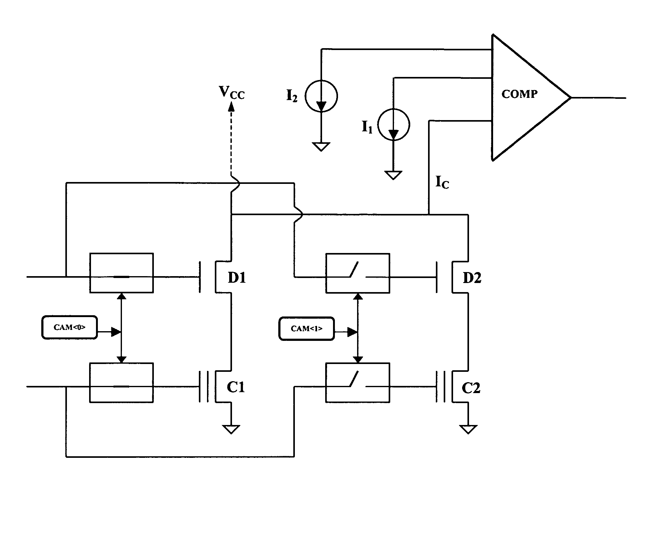
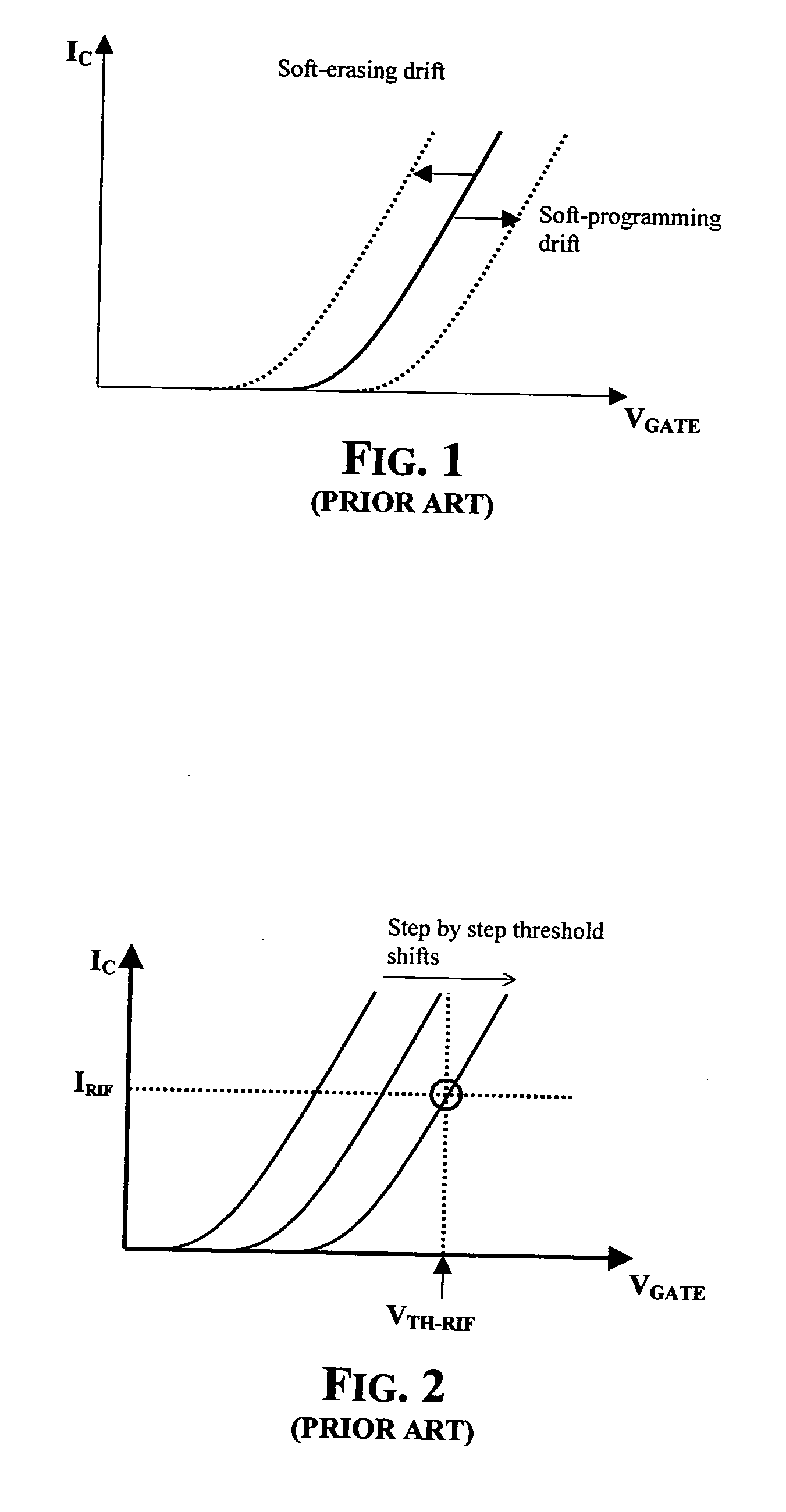
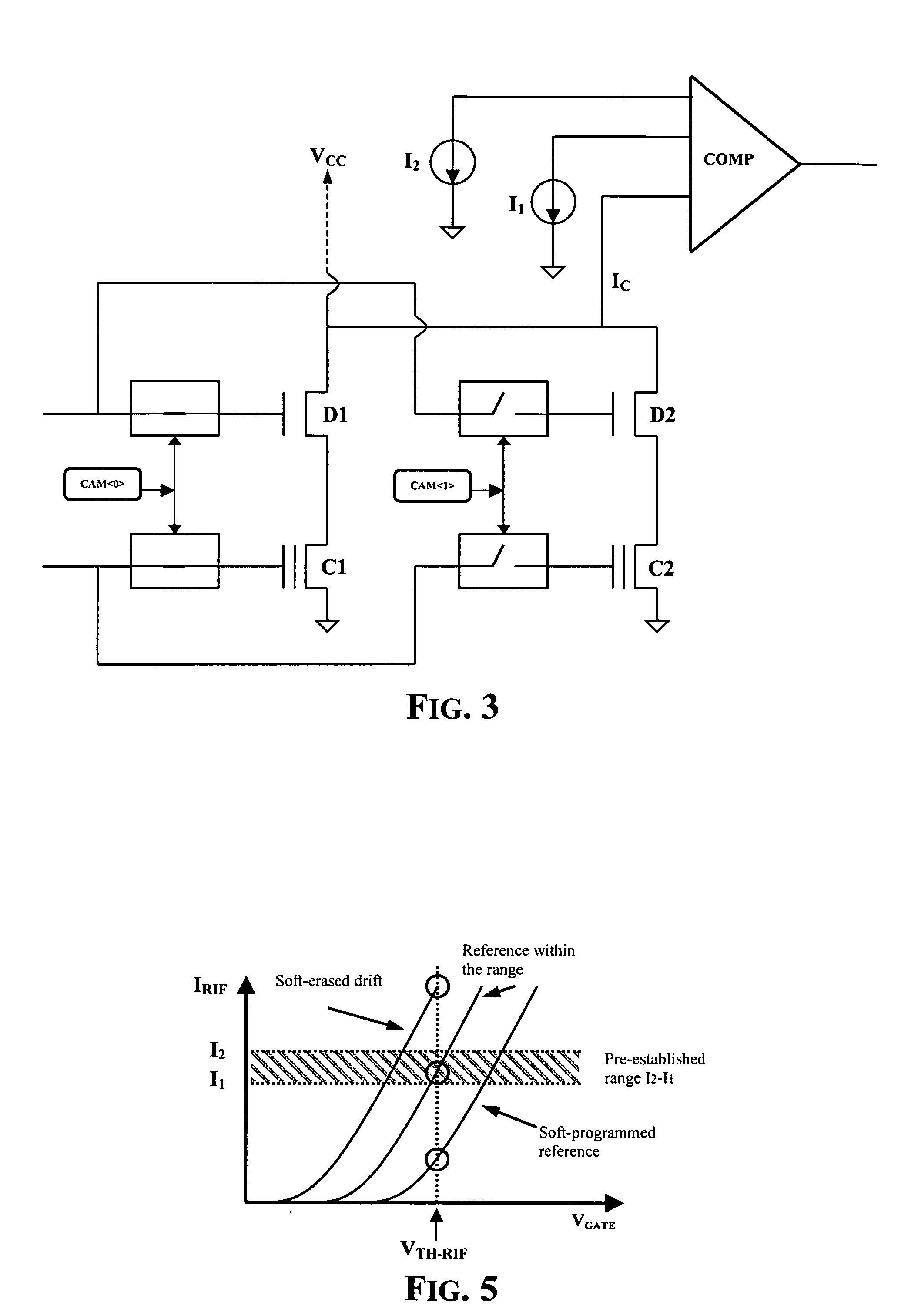
[0025] A basic scheme according to the preferred embodiment of a verification / substitution circuit of the invention, relative to a reference current path D1 and C1, is depicted in FIG. 3. The reference current path includes a decoding transistor D1 and a cell C1 connected in series to each other. The transistor D1 and the cell C1 are generally depicted for illustrative purposes as an insulated gate MOSFET. The verification / substitution circuit further comprises a second (redundant) reference current path D2, C2. The second reference current path is identical to the first reference current path, and is substituted for the first reference current path when for any reason the current Ic absorbed by the first reference current path is no longer in a pre-established design range [I1, I2]

[0026] The circuit includes a window comparator that compares the current Ic flowing in the reference current path D1, C1 with a pair of pre-established thresholds I1, I2. The window comparator outputs a ...


PUM


Abstract

A circuit verifies and substitutes a defective reference cell of a memory device that includes at least one reference current path including the reference cell and a decoding transistor connected in series. The circuit includes at least one redundant reference current path identical to the at least one reference current path and in parallel therewith. A connection circuit connects in a mutually exclusive way control terminals of the decoding transistor and reference cell of the at least one reference current path to a node or control terminals of the decoding transistor and reference cell of the at least one redundant reference current path to the node. The connecting is based upon a logic signal. A window comparator is coupled to the reference current path for comparing a current therein with a pair of upper and lower thresholds, and outputs the logic signal for the connection circuit based upon the comparison.

Description

FIELD OF THE INVENTION [0001] The invention relates in general to semiconductor memory devices, and more particularly, to a method and a circuit for verifying and eventually substituting defective reference cells of a memory device. BACKGROUND OF THE INVENTION [0002] A memory device comprises an array of cells organized in rows and columns singularly addressable through wordlines and bitlines. Each memory cell may comprise an insulated gate MOSFET including a source terminal connected to ground, a drain terminal connected to a decoding transistor of a respective bitline, and a gate connected to a wordline. [0003] An important field of application of the invention is to non-volatile FLASH memory devices. For this reason, reference will be made to these types of memory devices, although the invention may be applied to semiconductor memory devices in general other than FLASH memory devices. [0004] In FLASH memory devices it may be important to ensure reliability in writing and reading ...

Claims


Application Information

Patent Timeline
IPC IPC(8): G11C16/04G11C29/24
CPCG11C29/24
Inventor MARTINES, IGNAZIOTORRISI, DAVIDE
Owner MICRON TECH INC
Why Eureka
Try Eureka