

Optical device and method for fabricating the same
a technology of optical devices and optics, applied in the field of optical devices, can solve the problems of not providing a satisfactory high integration, and achieve the effect of high integration and small total thickness
- Summary
- Abstract
- Description
- Claims
- Application Information
AI Technical Summary
Benefits of technology
Problems solved by technology
Method used
Image

Examples
first embodiment
—Structure of Optical Device—
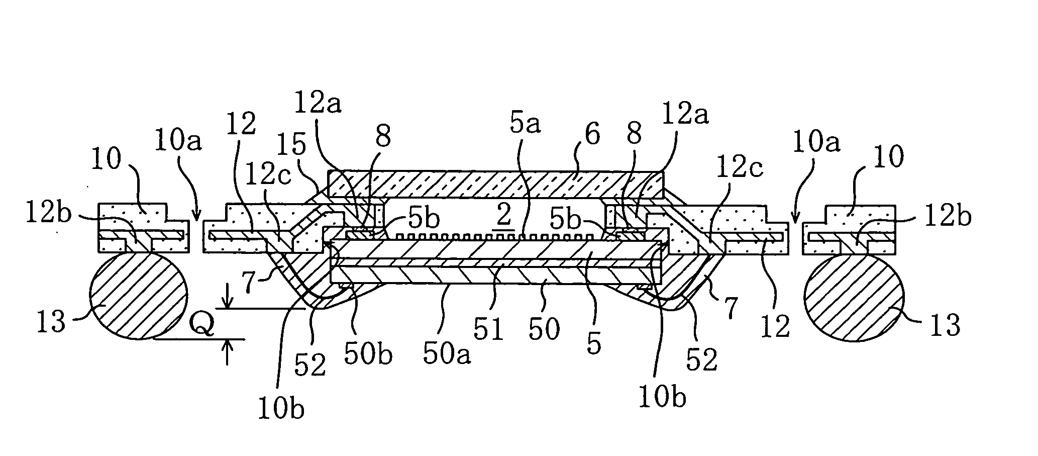
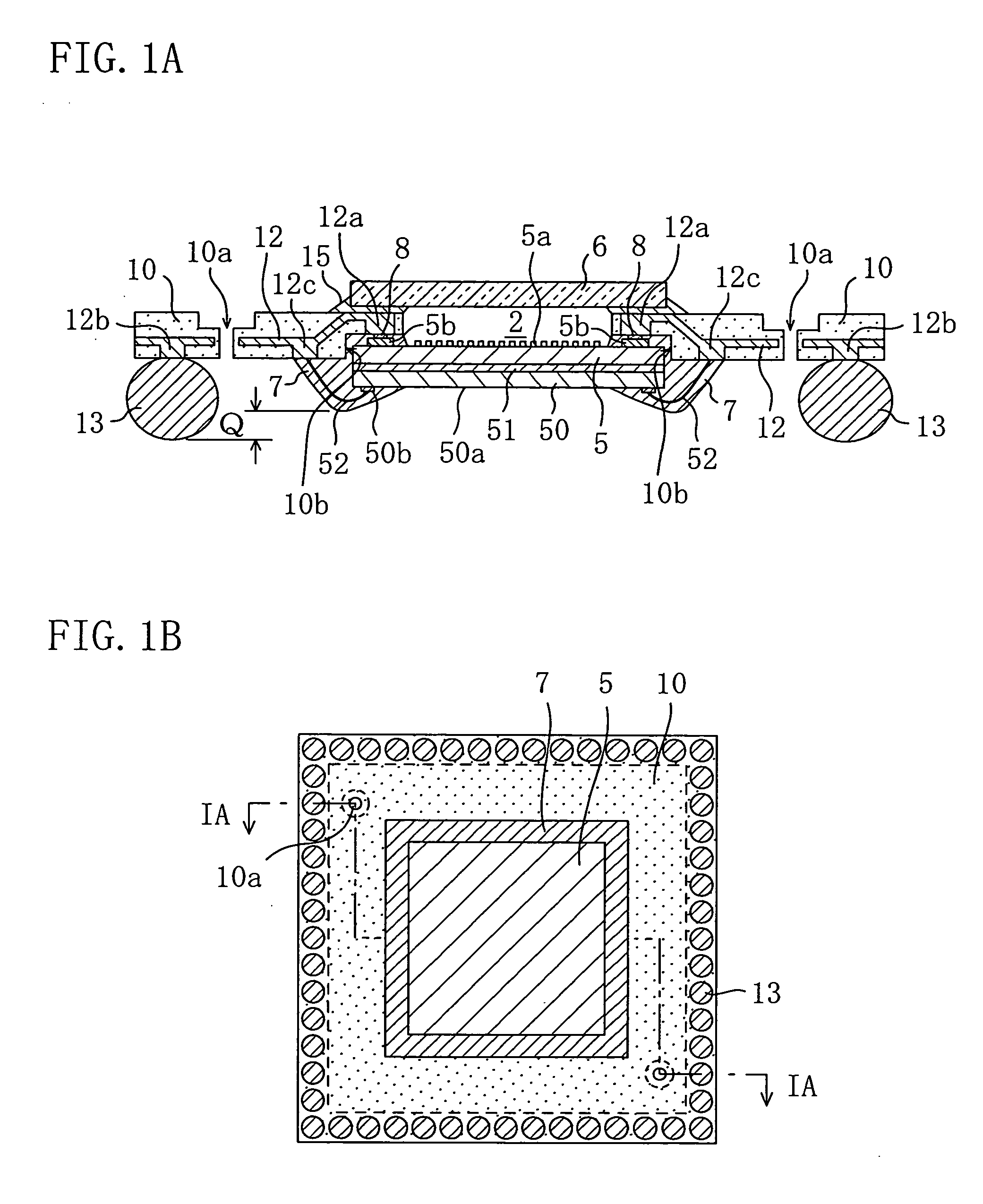
[0033]FIG. 1A is a sectional view of an optical device of a first embodiment, which is taken along the line IA-IA in FIG. 1B, and FIG. 1B is a backside view of the optical device. Note that FIGS. 1A and 1B are illustrated on different scales.
[0034] Referring to FIGS. 1A and 1B, the optical device of the first embodiment includes a base 10, an optical element chip 5, an integrated circuit chip 50, a window member 6, and a solder ball 13. The base 10 of frame shape is made of plastic resin such as epoxy resin and has an opening 2 in its center portion. The optical element chip 5 is attached to the lower surface of the base 10. The integrated circuit chip 50 is disposed on the back surface of the optical element chip 5 with an insulator layer 51 of adhesive interposed therebetween. The window member 6 is a translucent member made of glass and attached to the upper surface of the base 10 so that the member faces the optical element chip 5 with the opening 2...
second embodiment
[0068]FIG. 4A is a sectional view of an optical device of a second embodiment, which is taken along the line IVA-IVA in FIG. 4B, and FIG. 4B is a backside view of the optical device. Note that FIGS. 4A and 4B are illustrated on different scales.
[0069] Referring to FIGS. 4A and 4B, the optical device of the second embodiment includes a base 10, an optical element chip 5, an integrated circuit chip 50, a hologram 40, and a solder ball 13. The base 10 of frame shape is made of plastic resin such as epoxy resin and has an opening 2 in its center portion. The optical element chip 5 is attached to the lower surface of the base 10. The integrated circuit chip 50 is disposed on the back surface of the optical element chip 5 with an insulator layer 51 of adhesive interposed therebetween. The hologram 40 is a translucent member made of optical resin or the like and attached to the upper surface of the base 10 so that the hologram faces the optical element chip 5 with the opening 2 interposed...
third embodiment
—Structure of Optical Device—
[0084]FIG. 5A is a sectional view of an optical device of a third embodiment, which is taken along the line VA-VA in FIG. 5B, and FIG. 5B is a backside view of the optical device. Note that FIGS. 5A and 5B are illustrated on different scales.
[0085] Referring to FIGS. 5A and 5B, also in the optical device of the third embodiment, as in the case of the first embodiment, the internal terminal portion 12a of each wire 12 is bent up and the shoulder 10b is formed in a region of the lower surface of the base 10 surrounding the opening 2. That is to say, the region of the base 10 surrounding the opening 2 is thin, whereby the optical element chip 5 is bent up. The wires 12 are bent up so that the internal terminal portion 12a of each wire is positioned above other portions, and the lower surface of the base 10 is formed with the shoulder 10b whose upper level is on its upper region surrounding the opening 2. Around the internal terminal portion 12a, the upper ...
PUM
| Property | Measurement | Unit |
|---|---|---|
| thickness | aaaaa | aaaaa |
| thickness | aaaaa | aaaaa |
| length | aaaaa | aaaaa |
Abstract
Description
Claims
Application Information