Semiconductor package and method for fabricating the same

a technology of semiconductors and packages, applied in semiconductor devices, semiconductor/solid-state device details, electrical apparatus, etc., can solve the problems of affecting the appearance of the package, limiting the density and number of solder balls that can be and undesirably increasing the fabrication cost, so as to improve the bonding reliability, eliminate the drawbacks of encapsulant flash, and increase the density of solder balls implanted on the substrate

Inactive Publication Date: 2005-11-17
SILICONWARE PRECISION IND CO LTD
View PDF2 Cites 20 Cited by
  • Summary
  • Abstract
  • Description
  • Claims
  • Application Information

AI Technical Summary

Benefits of technology

[0015] The above finger holes in the core layer are formed by laser drilling. By a material selectivity characteristic of laser, the laser drilling technique can avoid damage to the bond fingers on the first circuit layer. The through opening in the core layer is formed by using a router. And the first opening of the first circuit layer and the second opening of the second circuit layer are formed by a conventional etching technique.
[0016] In addition, the core layer is further formed with a plurality of conductive vias for electrically connecting the first and second circuit layers to each other. A nickel(Ni) / gold(Au) layer is plated on the bond fingers respectively so as to enhance the bonding reliability between the bonding wires and the bond fingers.
[0017] Accordingly, by provision of the first and second openings of the first and second circuit layers respectively and the plurality of finger holes in the core layer in the present invention, the bonding wires are completely received in the through opening of the substrate, such that the encapsulant for encapsulating the bonding wires does not protrude out of the substrate. This allows the density of solder balls implanted on the substrate to be increased, and eliminates the drawbacks of encapsulant flash and difficulty in standardizing the mold used for fabricating the encapsulant. Moreover, in the present invention, the mechanical strength and supportability of the bonding wires can be improved. Thus the problems in the prior art can be solved by the present invention.

Problems solved by technology

However, since loops of the gold wires and the second encapsulant for encapsulating the gold wires protrude from the lower surface of the substrate, in order to fabricate appropriate second encapsulants, it needs to prepare different types of molds corresponding to different sizes and structures of openings in the substrates, which would undesirably increase the fabrication cost.
Moreover, in order to completely encapsulate the gold wires, the second encapsulant may occupy relatively much area on the substrate, thereby limiting the density and number of solder balls that can be implanted on the substrate.
In addition, since the first encapsulant and the second encapsulant are not completely symmetric to each other, the upper and lower molds may not firmly clamp the substrate, thereby leading to flash of the second encapsulant on the lower surface of the substrate.
This not only affects the appearance of the package but also may cover ball pads on lower surface of the substrate, which would adversely affect the ball-implanting process and degrade the electrical performance of the solder balls formed on the ball pads.
The flash problem is thus considered as a significant drawback in the prior art.

Method used


Image

  • Semiconductor package and method for fabricating the same
  • Semiconductor package and method for fabricating the same
  • Semiconductor package and method for fabricating the same

Examples


Embodiment Construction

[0023] Preferred embodiments of a semiconductor package and a method for fabricating the same proposed in the present invention are described in detail as follows with reference to FIGS. 3A to 3I and FIGS. 4A to 4D, wherein FIGS. 3A to 3I show a fabrication method of a substrate used in the semiconductor package.

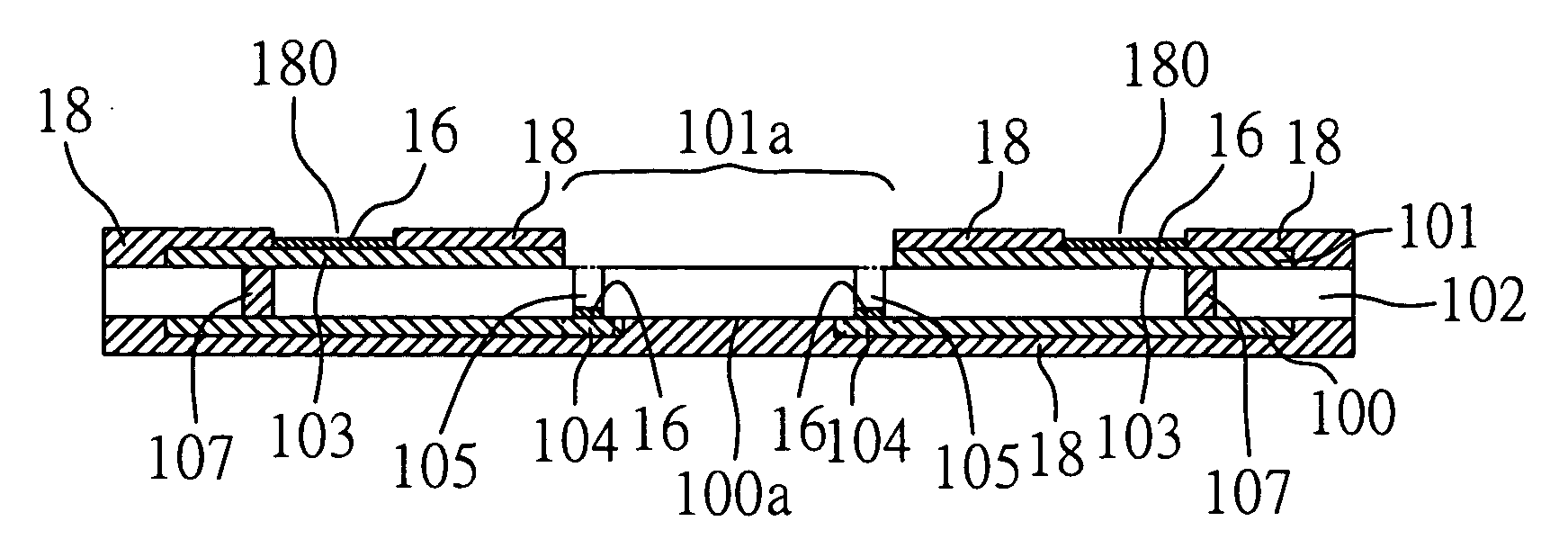
[0024] First, referring to FIG. 3A, a dual-layer substrate 10, such as a copper clad laminate (CCL) substrate, is prepared. This substrate 10 comprises a first copper circuit layer 100; a second copper circuit layer 101; an insulating core layer 102 formed between the first and second circuit layers 100, 101, making the first and second circuit layers 100, 101 separated by the core layer 102; and a plurality of conductive vias 107 formed in the core layer 102, for electrically connecting the first and second circuit layers 100, 101 to each other. Then, referring to FIG. 3B, the first and second circuit layers 100, 101 are subjected to a patterning process including exposure...


PUM


Abstract

A semiconductor package and a method for fabricating the same are proposed. A substrate having a first circuit layer, a second circuit layer, and a core layer formed between the first and second circuit layers is provided. At least one second opening is formed on the second circuit layer. At least one first opening is formed on the first circuit layer corresponding to the second opening. A plurality of finger holes corresponding to bond fingers on the first circuit layer are formed in the core layer. A through opening is formed in the core layer and communicates with the first and second openings. At least one chip is mounted on the first circuit layer and covers the first opening, with its active surface being exposed to the first opening. An encapsulant is formed to fill the first and second openings and the through opening and encapsulate the chip.

Description

FIELD OF THE INVENION [0001] The present invention relates to semiconductor packages and fabrication methods thereof, and more particularly, to a window ball grid array (WBGA) semiconductor package with an improved yield, and a method for fabricating the semiconductor package. BACKGROUND OF THE INVENTION [0002] A window ball grid array (WBGA) semiconductor package employs an advanced type of BGA packaging technology, wherein at least one opening is formed through a substrate, and a semiconductor chip is mounted on the substrate in an upside-down manner that an active surface of the chip faces downwards and covers the opening of the substrate, allowing the chip to be electrically connected to a lower surface of the substrate via a plurality of gold wires received in the opening. Such package structure can effectively reduce the length of gold wires and improve the quality of electrical communication between the chip and substrate, which thus has been widely applied to DRAM (dynamic r...

Claims


Application Information

Patent Timeline
Patent Type & Authority Applications(United States)
IPC IPC(8): H01L21/56H01L21/60H01L23/13H01L23/28H01L23/31H01L23/498
CPCH01L21/561H01L2924/01033H01L23/3128H01L23/49822H01L24/45H01L24/48H01L24/97H01L2224/45144H01L2224/48091H01L2224/4824H01L2224/484H01L2224/48599H01L2224/73215H01L2224/97H01L2924/01005H01L2924/01006H01L2924/01028H01L2924/01029H01L2924/01078H01L2924/01079H01L2924/01082H01L2924/014H01L2924/15311H01L2224/32225H01L23/13H01L2924/00014H01L2224/83H01L2224/85H01L2924/00H01L2924/181H01L2924/12042H01L2924/00012
Inventor WANG, YU-POHUANG, CHIEN-PINGHSIAO, CHENG-HSU
Owner SILICONWARE PRECISION IND CO LTD
Why Eureka
Try Eureka