Matrix display device

a display device and matrix technology, applied in the field of matrix display devices, can solve the problems of not being suitable or intended for use in matrix display devices, unable to use known electron guns, severe problems, etc., and achieve the effects of large viewing angle, large variation in the amount of electrons drawn from the cavity, and large viewing angl

Inactive Publication Date: 2005-11-17
KONINKLIJKE PHILIPS ELECTRONICS NV
View PDF3 Cites 0 Cited by
  • Summary
  • Abstract
  • Description
  • Claims
  • Application Information

AI Technical Summary

Benefits of technology

[0008] High efficiency and a large viewing angle are obtained when a phosphor display screen is used. Supplying an oscillating (usually RF frequency) AC voltage generates an electron cloud in the cavities by multiplication due to secondary electron emission. The intensity of said cloud shows as the inventors have seen, probably because the cloud is in saturation, little variation between cavities or in time. Thus variations in the amount of electrons drawn from the cavities are relatively small, reducing problems due to variation in intensity. Furthermore detrimental thermal effects are much smaller than when thermionic cathodes are used. Whereas when cathodes for generating electrons are used heat generation is localized (the cathodes form “hot spots”) and also differs from one cathode to the next, heat generation in the device in accordance with the invention heat generation is generally smaller and evenly distributed over the planar arrangement of cavities, leading to a more evenly distributed heat generation which heat is also more easily carried off, if needed. This strongly reduces the occurrence of differences in temperature and thereby also of thermal drift.
[0009] It is observed that generation of secondary electrons by a RF field is a known effect. The effect causes problems, sometimes severe problems, in such devices as klystrons and standing wave tubes. In U.S. Pat. No. 3,201,640 an electron gun for a CRT is described in which a set of concave electrodes are used between which an oscillating electrical field is provided. However, in this known device the object is to provide a single pencil-like focused high-intensity electron beam in a standard cathode ray tube. In such a device the heat generation is still localized, large thermal differences and thermal drift still occur and, furthermore, the known electron gun cannot be used, nor is suitable for or intended for use in a matrix display device.
[0010] Preferably the arrangement of cavities comprises elongated cavities extending in a direction parallel to a row or a column, the elongated cavities being separated by a wall. Such an arrangement, compared with arrangements where a separate cavity is provided for each pixel, offers a simplification of the design. This also lowers the RF frequency which is advantageous since in general the lower the RF frequency the simpler the electronics may be.

Problems solved by technology

Furthermore detrimental thermal effects are much smaller than when thermionic cathodes are used.
The effect causes problems, sometimes severe problems, in such devices as klystrons and standing wave tubes.
In such a device the heat generation is still localized, large thermal differences and thermal drift still occur and, furthermore, the known electron gun cannot be used, nor is suitable for or intended for use in a matrix display device.

Method used


Image

  • Matrix display device
  • Matrix display device
  • Matrix display device

Examples


Embodiment Construction

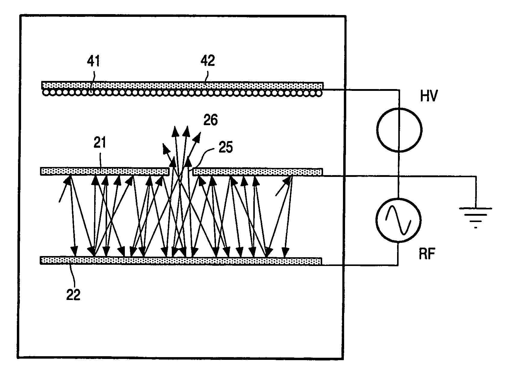
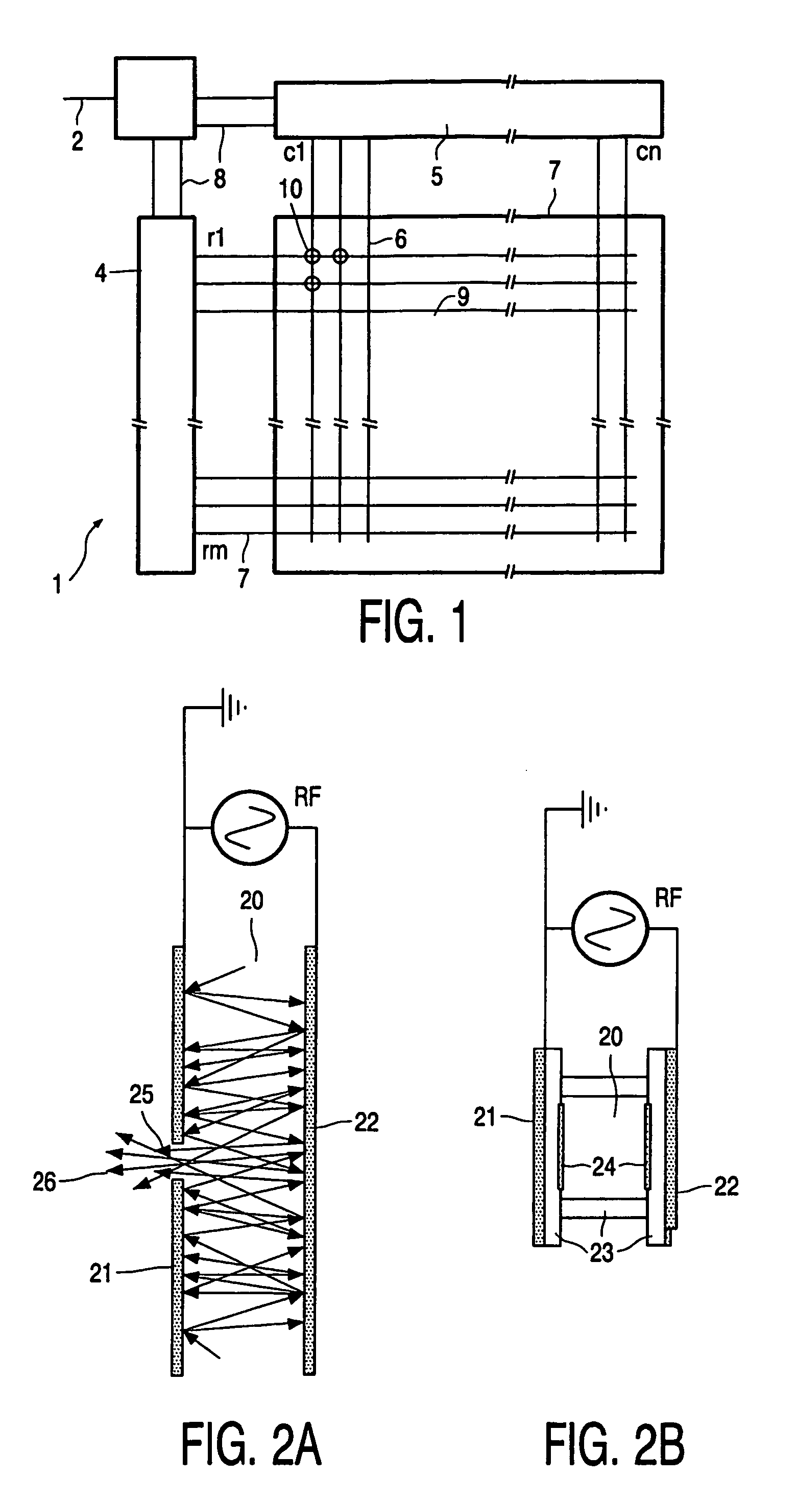
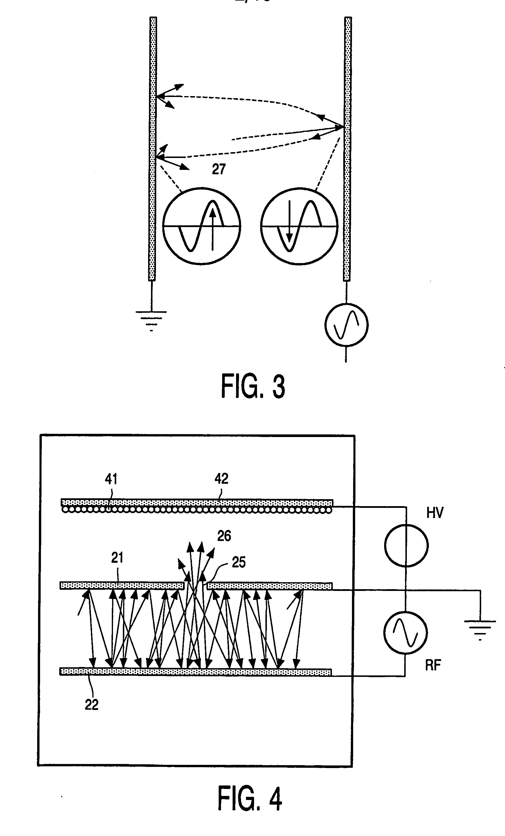
[0019]FIG. 1 shows schematically a highly simplified electric equivalent of a matrix display device 1. It comprises a number of row elements 7 and column elements 6 intersecting at a matrix of intersections 10. The row elements r1 to rm can be activated by means of a row driver 4, while the column electrodes c1 to cn are provided with data via a column driver 5. To this end, incoming data 2 can be first processed, if necessary, in a processor 3. Mutual synchronization between the row driver 4 and the data column driver 5 may take place.

[0020] Signals from the row driver 4 and the column driver 5 selectively activate an intersection 10. Usually a column element 6 comprises an electrode which acquires such a voltage with respect to an electrode of a row element 7 that the intersection is activated and thereby a pixel on a display screen associated with the relevant intersection is activated (or deactivated, but in any way a visible effect is generated in the pixel). This Figure shows...


PUM


Abstract

A matrix display device comprises cavities (20) having walls at least one of which is covered with a material (24) having a secondary emission coefficient of more than unity. The cavities form a planar arrangement substantially parallel to the display screen which has a phosphor display screen. The cavities are provided with electrodes (21, 215, 217, 5 22, 225, 228) and the display device has a circuit for supplying an oscillating AC voltage (Vr, VRF) to said electrodes (21, 215, 217, 22, 225, 228) for generating electrons within the cavities by secondary emission. The cavities (20) have apertures (25) facing the screen (41), and the display device has a circuit for selectively letting electrons generated within the cavities pass said apertures and accelerating electrons having passed said apertures to the phosphor display screen.

Description

FIELD OF THE INVENTION [0001] The invention relates to a matrix display device, having a flat display screen, comprising pixels arranged in rows and columns and a system having electrodes and an addressing circuit for addressing the pixels. [0002] Many such matrix displays are known and range from plasma display panels (PDPs), plasma-addressed liquid crystal panels (PALCs), liquid crystal displays (LCDs), to Polymer LEDs (PLEDs), to Electroluminescent (EL) displays to flat CRT devices in which electrons are generated, for instance by line cathodes. Such displays are used e.g., but not exclusively, for personal computers, television sets and so forth. Within the concept of the invention pixels are to be understood to be any addressable image elements. BACKGROUND OF THE INVENTION [0003] A matrix display device comprises a first set of elements (rows) extending in a first direction, usually called the row direction, and a second set of elements (columns) extending in a second direction...

Claims


Application Information

Patent Timeline
Patent Type & Authority Applications(United States)
IPC IPC(8): G09G1/20G09G3/22H01J3/02H01J17/49H01J29/48H01J31/12
CPCG09G1/20G09G3/22G09G2310/06H01J2329/46H01J29/482H01J31/127H01J29/481H01J31/12H01J31/10
Inventor DIJK, ROY VANDE ZWART, SIEBE TJERKVAN GORKOM, RAMON PASCALVAN DEN BRINK, HENDRIKUS BERNARDUS
Owner KONINKLIJKE PHILIPS ELECTRONICS NV
Why Eureka
Try Eureka