

AD conversion method and semiconductor device for use in physical quantity distribution detection
a conversion method and semiconductor technology, applied in the field of analog-to-digital-based conversion methods and semiconductor devices for physical quantity distribution detection, can solve the problem that the adjustment may not be necessarily conducted relating to the color, and achieve the effect of reducing the number of signal lines
- Summary
- Abstract
- Description
- Claims
- Application Information
AI Technical Summary
Benefits of technology
Problems solved by technology
Method used
Image

Examples
first embodiment
The Operation of the Solid-State Imaging Device
[0146]FIG. 4 is a timing chart for describing the signal acquisition differential process that is the basic operation in the column AD circuit 25 of the solid-state imaging device 1 of the first embodiment shown in FIG. 1.
[0147] For the scheme that converts the analog pixel signal sensed by each of the unit pixels 3 in the pixel portion 10 to the digital signal, for example, a scheme that obtains the count value corresponding to the magnitude of the reference component and the signal component is adopted in which a point is searched that matches the reference signal RAMP in a ramp waveform dropping by a predetermined tilt with each voltage of the reference component and the signal component in the pixel signal from the unit pixel 3, and the count clock counts the period from the point in time when the reference signal RAMP used in the comparison process is generated to the point in time when the electric signal in accordance with the ...
second embodiment
The Operation of the Pipeline Process
[0195]FIG. 6 is a timing chart for describing the basic operation in the column AD circuit 25 of the solid-state imaging device 1 of the second embodiment shown in FIG. 5. The AD conversion process in the column AD circuit 25 is the same as that of the first embodiment. Here, the detailed description will be omitted.
[0196] The second embodiment has the data storing portion 256 added to the configuration of the first embodiment, and the basic operations including the AD conversion process are the same as those of the first embodiment. However, before the operation of the counter portion 254 (t6), the count result in processing the previous row HX−1 is transferred to the data storing portion 256 based on the memory transfer instruction pulse CN8 from the communication and timing control portion 20.
[0197] In the first embodiment, pixel data cannot be output to outside the column processing portion 26 unless after the second time readout process i...
third embodiment
The Configuration of the Solid-State Imaging Device: Addition of Emerald Pixels
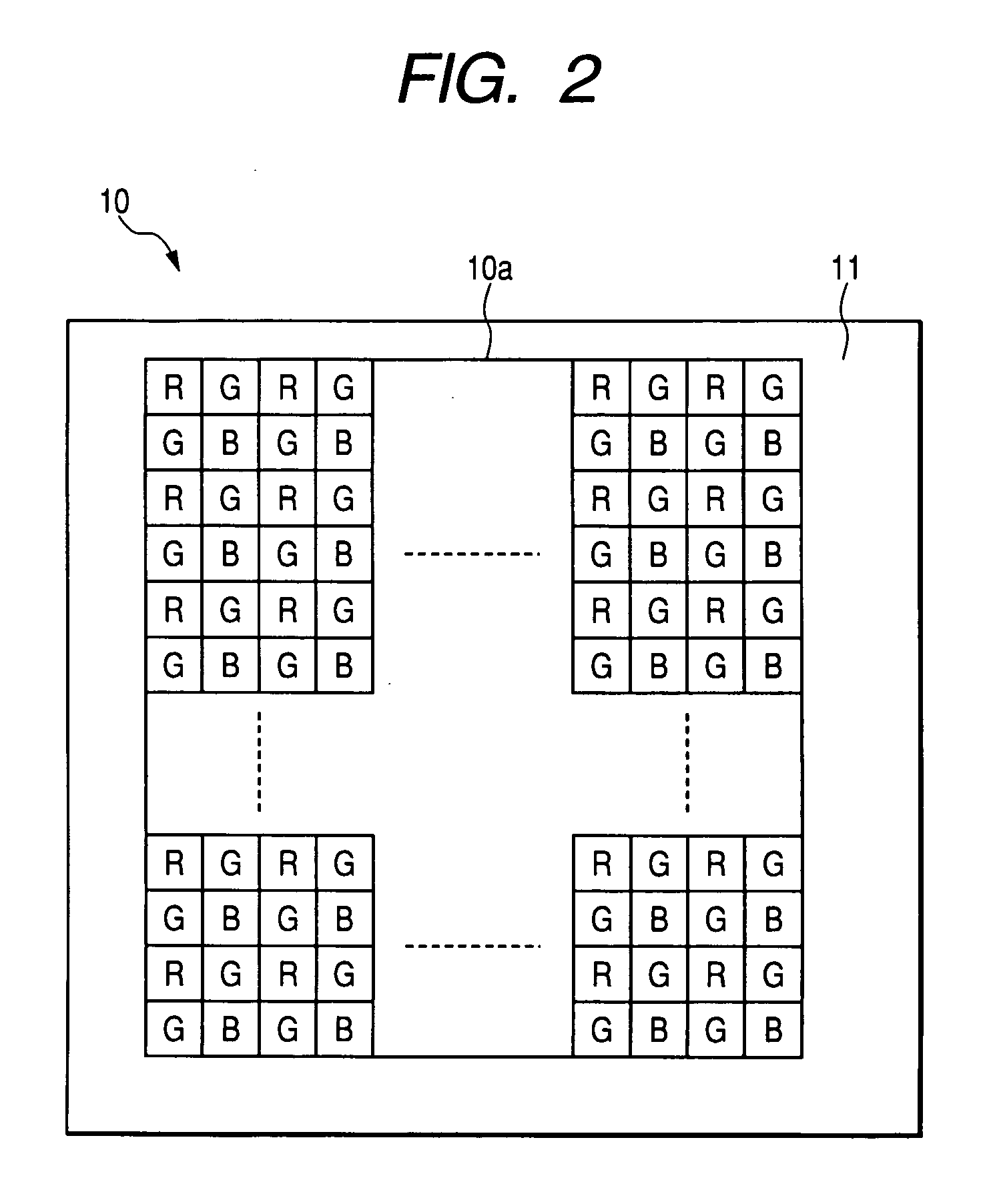
[0199]FIG. 7 is a diagram illustrating the outline configuration of a CMOS solid-state imaging device according to a third embodiment of the invention. The solid-state imaging device 1 of the third embodiment has a feature in that the color filter arrangement of the color separation filter is modified. More specifically, in the first and second embodiments, three color filters, red (R), green (G), and blue (B), are arranged in accordance with the basic form of the Bayer arrangement for the unit pixels 3 arranged in a square grid, but filter colors and the arrangement order thereof are not defined to the basic form of the Bayer arrangement. For example, the Bayer arrangement may be modified and complementary color filters or the other filter colors may be used.
[0200] For example, as shown in FIG. 7, a fourth color pixel which senses a fourth color (emerald: E) may be arranged instead of the second color ...
PUM
 Abstract
Description
Claims
Application Information