Method of manufacturing liquid crystal display

a liquid crystal display and manufacturing method technology, applied in the direction of instruments, semiconductor devices, optics, etc., can solve the problems of increased misalignment risk, more etc., and achieve the effect of increasing process cycle time and cost, and increasing misalignment risk

Active Publication Date: 2005-11-17
INNOLUX CORP
View PDF0 Cites 6 Cited by
  • Summary
  • Abstract
  • Description
  • Claims
  • Application Information

AI Technical Summary

Benefits of technology

[0008] The more photomasks used in manufacturing a TFT device, the more process cycle time and cost are incurred. Misalignment risk is also increased. Therefore, a method is required for manufacturing the thin film transistor and the peripheral CMOS transistor control circuit without involving a lot of photolithography processes. Moreover, a liquid crystal display structure with transmission regions and reflection regions is also required so that partial incident light can pass through a transmission region while other incident light can be reflected by a reflection region. Such a structure can be used in a darker environment.

Problems solved by technology

The more photomasks used in manufacturing a TFT device, the more process cycle time and cost are incurred.
Misalignment risk is also increased.

Method used


Image

  • Method of manufacturing liquid crystal display
  • Method of manufacturing liquid crystal display
  • Method of manufacturing liquid crystal display

Examples


Embodiment Construction

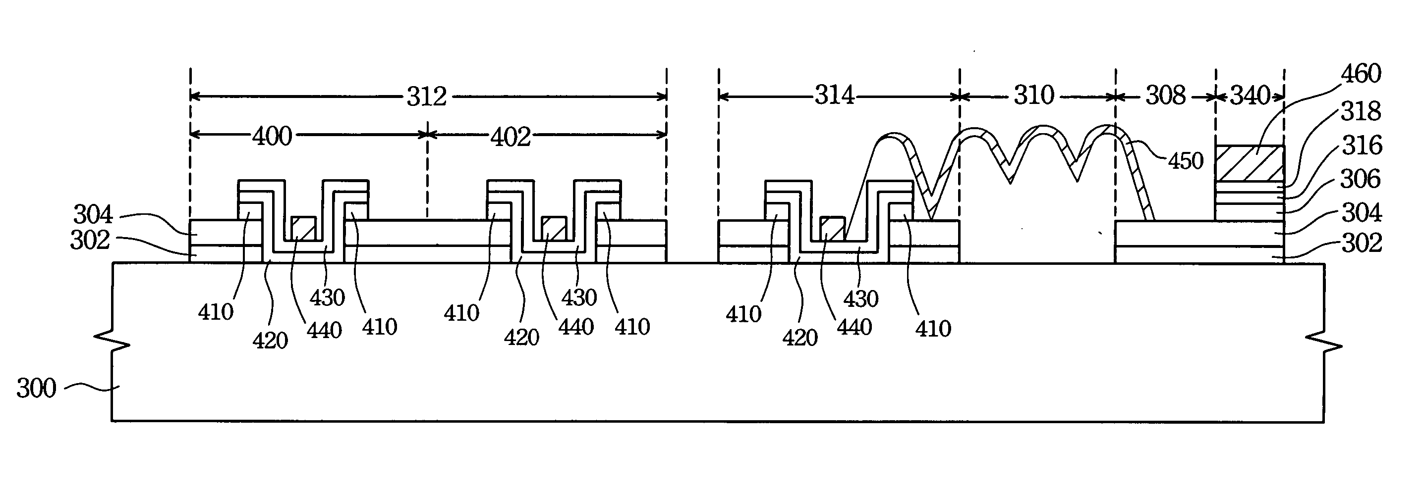
[0026] Without limiting the spirit and scope of the present invention, the method proposed in the present invention is illustrated with one embodiment of forming thin film transistors and the peripheral CMOS transistor control circuit in a TFT-LCD. Skilled artisans, upon acknowledging the embodiments, can apply the present invention to any kind of TFT apparatus to reduce the process cycle time and the cost required to manufacture the TFT-LCD. Moreover, according to the present invention, a TFT-LCD with transmission regions and reflection regions can also be formed by using the same photolithography process. In such a structure, partial incident light can pass through the transmission region while other incident light is reflected by the reflection region in order to maximize the light-utilization efficiency in the two regions. Therefore, this structure can be used in a darker environment. The usage of the present invention is not limited by the embodiment that follows.

[0027] The pr...


PUM

PropertyMeasurementUnit
thicknessaaaaaaaaaa
thicknessaaaaaaaaaa
thicknessaaaaaaaaaa

Abstract

A conductive layer, a metal layer and a doped layer are sequentially formed on a glass substrate. A CMOS circuit region, a transistor region, a reflective region, a transmission region and a capacitor region are defined. Next, a polysilicon layer and an insulating layer are formed to serve as a source/drain region, a channel region and a gate insulating layer. Then, a resin layer with a rough surface is formed. Next, a metal layer is formed to serve as a gate structure and a reflective electrode. Then, an ion implanting process is performed to form the source/drain structure of a PMOS. Then, a passivation layer is formed to define a transmission region. Finally, the metal layer and the doped layer are removed to expose the conductive layer.

Description

FIELD OF THE INVENTION [0001] The present invention relates to a method for manufacturing a liquid crystal display, and more particularly to a method for manufacturing a liquid crystal display having a reflection region and a transmission region. BACKGROUND OF THE INVENTION [0002] Liquid crystal displays (LCDs) have been widely applied in electronic products, such as digital watches and calculators, for a long time. With the advance of techniques for manufacture and design, the thin film transistor liquid crystal displays (TFT-LCDs) have been introduced into portable computers, personal digital assistants and color televisions, and have gradually replaced the kinescopes that are used for conventional displays. However, consequent of the TFT-LCD design rules trend toward large scale, there are a lot of problems and challenges, such as low yields and low throughput, in manufacturing and developing TFT-LCD apparatuses. [0003] In general, the TFT-LCD comprises a bottom plate on which I ...

Claims


Application Information

Patent Timeline
Patent Type & Authority Applications(United States)
IPC IPC(8): G02F1/1335G02F1/1362H01L21/00H01L21/77H01L21/84
CPCG02F1/133555H01L27/1214G02F1/13454H01L27/1288
Inventor CHEN, HSIN-MING
Owner INNOLUX CORP
Why Eureka
Try Eureka