Semiconductor device

Active Publication Date: 2005-11-24
RENESAS ELECTRONICS CORP
View PDF6 Cites 70 Cited by
  • Summary
  • Abstract
  • Description
  • Claims
  • Application Information

AI Technical Summary

Benefits of technology

[0024] Advantageous effects obtained by the invention disclosed in the present application will be explained in brief as follows:
[0025] It is possible to suppress crosstalk noise developed between two signals which are held in a relationship in which one si

Problems solved by technology

It has been discovered by the present inventors that there is a concern that, in a synchronous SRAM, the free running echo clock is outputted and operated even during a write operation, and an undesired data error occurs due to a change in the clock causing crosstalk of input data.
However, it is difficult to completely separate a data input/output terminal of the synchronous SRAM and an output terminal for the free running echo clock by application of the technique described in the patent document 2.
Such separation leads to a shift

Method used


Image

  • Semiconductor device
  • Semiconductor device
  • Semiconductor device

Examples


Embodiment Construction

>

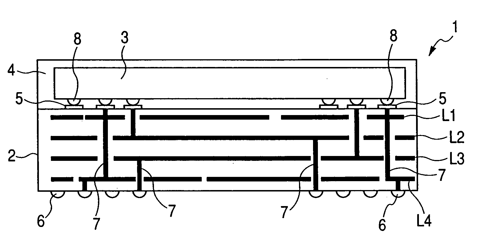
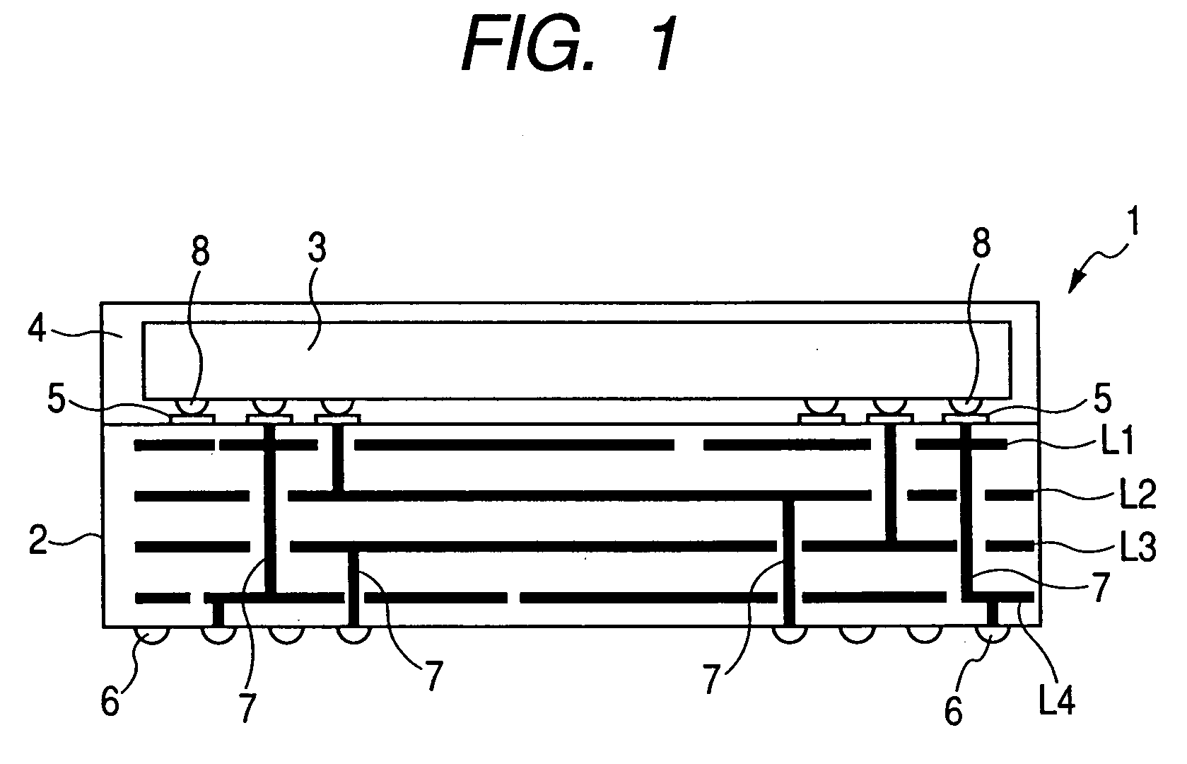
[0052] A cross-sectional view of a semiconductor device according to the present invention is illustrated in FIG. 1. The semiconductor device 1 has a CSP configuration in which a semiconductor chip 3 is mounted over a wiring board (called a “package substrate”) 2. The surface of the semiconductor chip 3 is molded with a resin 4. The package substrate 2 has one surface formed with a plurality of chip connecting electrodes connected to the semiconductor chip 3, e.g., pad electrodes 5, and the other surface is formed with a plurality of external connecting electrodes, e.g., solder ball electrodes 6. In the figure, the package substrate 2 is configured as a ceramic substrate having wiring layers L1 through L4 corresponding to four layers. In order to connect the pad electrodes 5 to their corresponding solder ball electrodes 6, the package substrate 2 has required wirings formed in the wiring layers L1 through L4, and vias 7 that connect wirings among the wiring layers L1 through L4. Th...


PUM


Abstract

A wiring board includes a plurality of wiring layers, and one surface formed with a plurality of chip connecting electrodes and another surface formed with a plurality of external connecting electrodes of a semiconductor device. The wiring board has wiring layers and vias. The plurality of chip connecting electrodes include first chip connecting electrodes, each used for a first signal whose logic value changes, and second chip connecting electrodes, each used for a second signal that changes after a change timing of the first signal. A wiring layer in which wiring routing of paths extending from the first chip connecting electrodes to their corresponding first external connecting electrodes is performed, and a wiring layer in which wiring routing of paths extending from the second chip connecting electrodes disposed adjacent to the first chip connecting electrodes to their corresponding second external connecting electrodes is performed, are made different from each other.

Description

CROSS-REFERENCE TO RELATED APPLICATION [0001] The present application claims priority from Japanese patent application No. 2004-153086, filed on May 24, 2004, the content of which is hereby incorporated by reference into this application. BACKGROUND OF THE INVENTION [0002] The present invention relates in general to a semiconductor device having a CSP (Chip Size Package) configuration, or the like, wherein a semiconductor chip is mounted over a wiring board, and, more particularly, the invention relates to a technique for improving noise caused by a wiring routing arrangement provided over a wiring board, e.g., a technique that is effective when applied to a synchronous SRAM (Static Random Access Memory), or the like, that is memory-operated in a DDR (Double Data Rate) mode. [0003] A clock synchronized memory, such as a synchronous SRAM, outputs a clock signal that is synchronized with a data output timing in order to indicate timing provided to determine read data to an access main...

Claims


Application Information

Patent Timeline
IPC IPC(8): H01L23/12H01L23/04H01L23/498H01L29/40H05K1/00H05K1/02H05K1/11
CPCH01L23/49827H01L23/49838H01L2224/16225H01L2924/01078H01L2924/15173H05K2201/10674H01L2924/3025H05K1/0237H05K1/0298H05K1/112H05K2201/09227H01L2924/15311H01L2924/181H01L2924/00012A01G9/02E02D29/0241E02D29/0266E02D2600/20
Inventor YOSHIKAWA, YASUHIROSUWA, MOTOONAMBU, HIROAKI
Owner RENESAS ELECTRONICS CORP
Why Eureka
Try Eureka