Substrate for solder joint

Inactive Publication Date: 2005-11-24
UTAC HEADQUARTERS PTE LTD
View PDF4 Cites 14 Cited by
  • Summary
  • Abstract
  • Description
  • Claims
  • Application Information

AI Technical Summary

Benefits of technology

[0015] The foregoing substrate for solder joint yields significant benefits. First, the pads can be arranged in a fine pitch manner on the substrate. Due to the hollow portions being formed internally through the pads and free of contact with the periphery of the pads, the etching process for forming the internal hollow portions, not etching the pads from the periphery thereof, would be performed more easily and accurately than that for etching the conventional trace terminals from the periphery thereof in the prior art even if the pads are closely spaced from each other. Further, the substrate provides a flash prevention mechanism. When the substrate is subject to a molding process in which a resin compound such as epoxy resin is applied over the substrate to form an encapsulation body, an elevated portion of the solder mask situated around the opening and on the pad is elevated in height by the thickness of the underneath pad. As a result, during molding, when the resin compound flows to the elevated portion, it would decrease its flowing speed and fails to enter the opening and flash over the exposed part of the pad or core layer, such that the exposed pad and core

Problems solved by technology

This would desirably increase contact area between the substrate and the solder ball (or bump), thereby securing

Method used


Image

  • Substrate for solder joint
  • Substrate for solder joint
  • Substrate for solder joint

Examples


Embodiment Construction

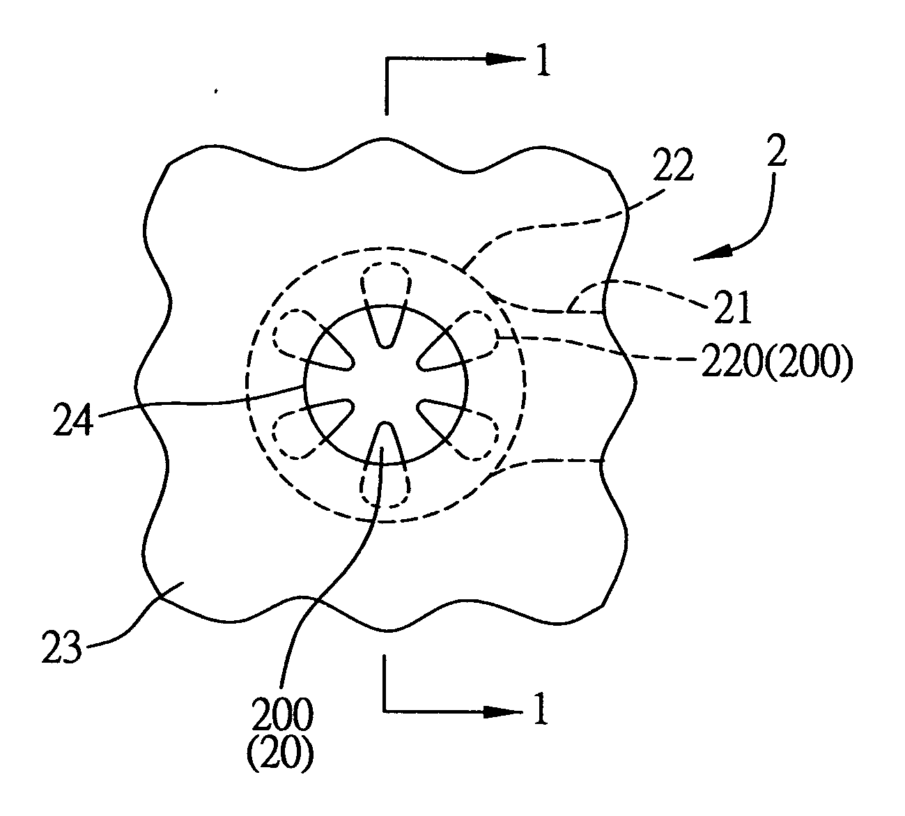
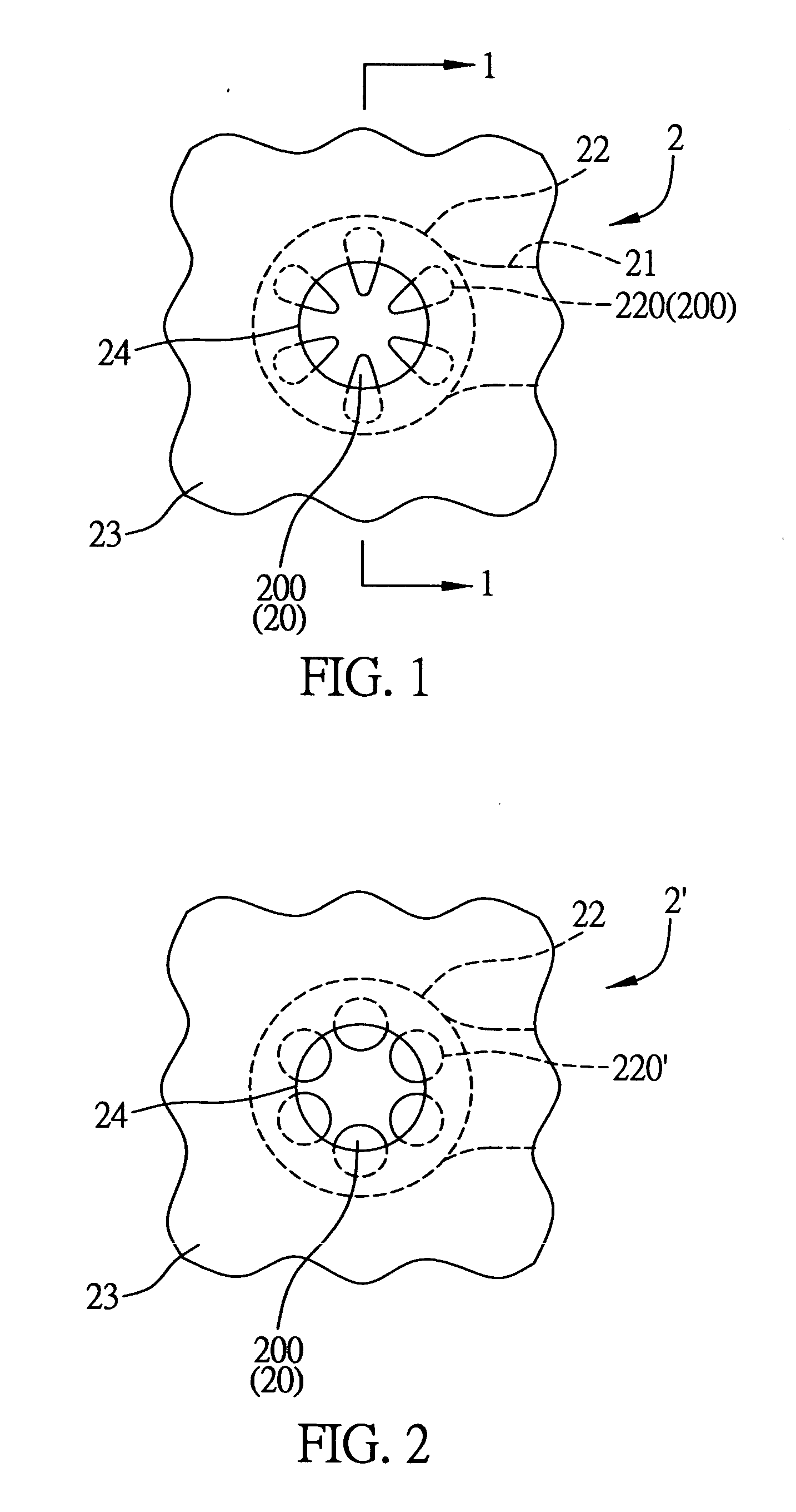
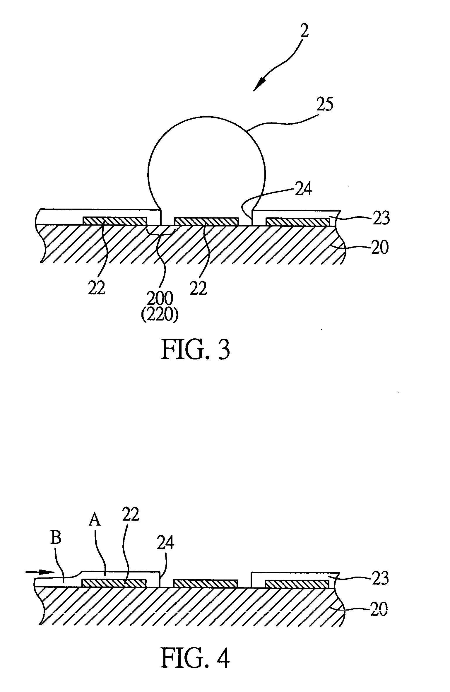
[0025] The preferred embodiments of a substrate for solder joint proposed in the present invention are described with reference to FIGS. 1 to 4.

[0026] As shown in FIGS. 1 and 3, a substrate 2 for solder joint according to the invention comprises: a core layer 20; at least one conductive trace 21 formed on a surface of the core layer 20 and having a circular terminal 22 that serves as a pad 22 (designated by the same reference numeral as the terminal 22) through which a plurality of hollow portions 220 are formed and thereby expose predetermined portions 200 of the core layer 20 underneath the pad 22; and a solder mask 23 applied over the surface of the core layer 20 for covering the conductive trace 21, and formed with at least one opening 24 via which part of the pad 22 and part of each predetermined portion 200 of the core layer 20 are exposed, such that a solder ball 25 (or bump) can be bonded to the exposed part of the pad 22 and the exposed part of each predetermined portion 2...


PUM


Abstract

A substrate for solder joint is provided, including: a core layer; at least one conductive trace formed on the core layer and having a circular terminal as a pad through which a plurality of hollow portions are formed and expose predetermined portions of the core layer underneath the pad, wherein the hollow portions are arranged at equal intervals and spaced from a periphery of the circular pad; and a solder mask for covering the conductive trace and having at least one opening bordered across each of the hollow portions of the pad, such that part of the pad and part of each of the predetermined portions of the core layer are exposed via the opening, to allow a conductive element to be bonded to the exposed part of the pad and the exposed part of the predetermined portions of the core layer in the opening of the solder mask.

Description

FIELD OF THE INVENTION [0001] The present invention relates to substrates for solder joint, and more particularly, to a substrate having at least one bond pad thereon to which a solder ball or bump can be bonded. BACKGROUND OF THE INVENTION [0002] Substrate is a critical component for a semiconductor package, which usually serves as a chip carrier whose one side is mounted with at least one semiconductor chip that is electrically connected to conductive traces formed on the substrate. On an opposite side of the substrate there are also formed a plurality of conductive traces that are electrically coupled to the conductive traces on the side having the chip by means of conductive vias penetrating through the substrate. BGA (ball grid array) package is characterized in bonding an array of solder balls to the side opposite to the chip-mounting side of the substrate and electrically connecting the solder balls to the conductive traces on the substrate, and the solder balls can be furthe...

Claims


Application Information

Patent Timeline
IPC IPC(8): H01L23/48H01L23/485H01L23/498H05K1/11H05K3/34
CPCH01L23/49816H01L2224/05567H01L2224/0401H01L2224/05552H01L2224/16H01L2224/81801H01L2924/01005H01L2924/01029H01L2924/01082H01L2924/014H05K1/111H05K3/3452H05K3/3457H05K2201/0969H05K2201/0989H05K2201/099H01L24/05H01L2924/01033H01L2224/05551H01L24/12H01L2224/0235H01L2224/02351H01L2224/05548Y02P70/50
Inventor KIM, SUNG-JIN
Owner UTAC HEADQUARTERS PTE LTD
Why Eureka
Try Eureka