

Bonding method, bonding stage and electronic component packaging apparatus
- Summary
- Abstract
- Description
- Claims
- Application Information
AI Technical Summary
Benefits of technology
Problems solved by technology
Method used
Image

Examples
first embodiment
(First Embodiment)
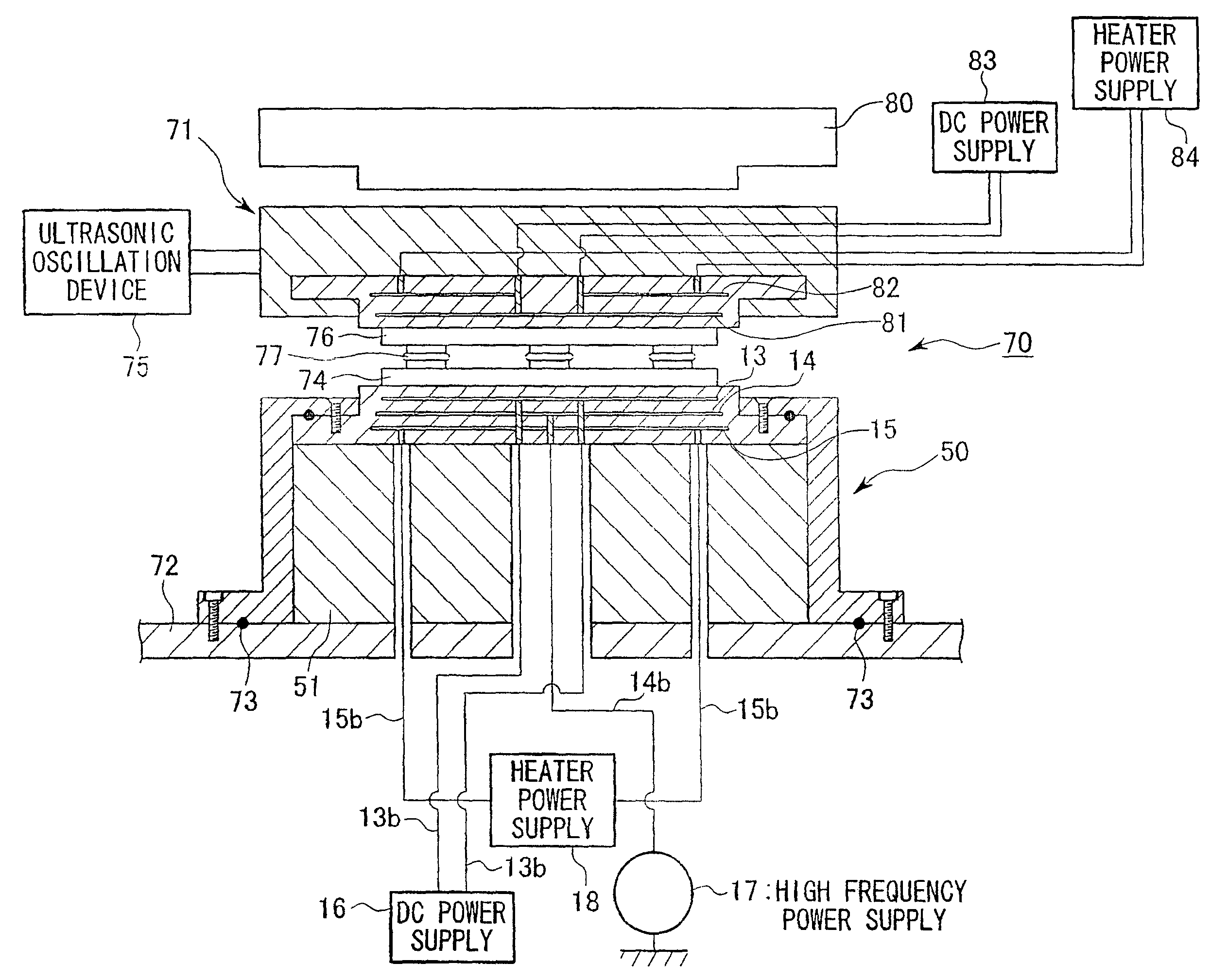
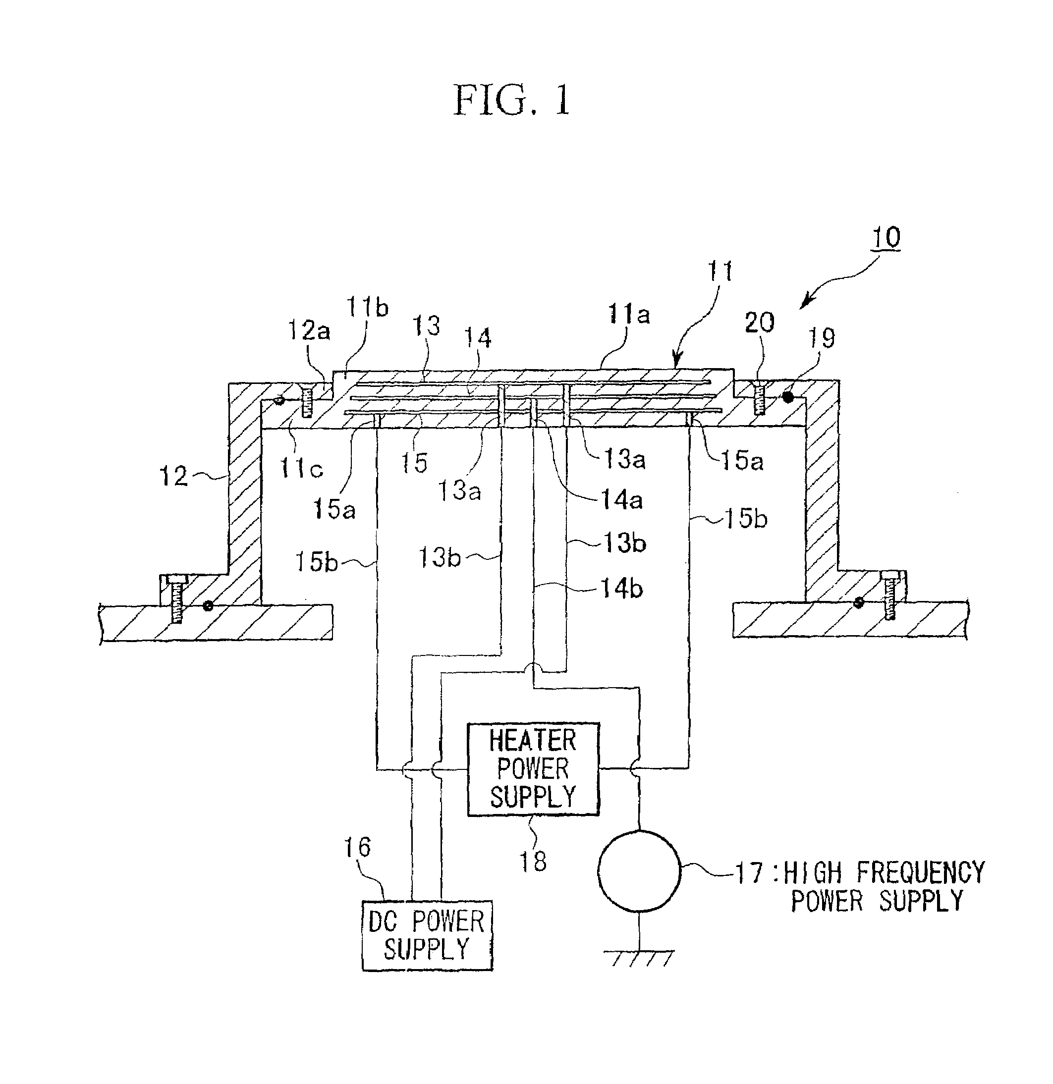
[0061]FIG. 1 is a view showing a first embodiment of a bonding stage that may be favorably used to implement the above described flip chip bonding method. In FIG. 1, the reference numeral 10 is a bonding stage. The bonding stage 10 is provided with a placement base 11 (i.e., a placement member) that has a placement surface 11a on which is placed either a circuit substrate (i.e., a processed substrate (not shown)) on which a predetermined circuit pattern has been formed or a semiconductor chip (i.e., an electronic component (not shown)). The bonding stage 10 is also provided with a supporting member 12 having a cylindrical configuration that supports the placement base 11.
[0062]The placement base 11 is substantially disk shaped and has a top disk portion 11b on an upper surface thereof, and a bottom disk portion 11c having a larger diameter than the top disk portion 11b on the bottom surface thereof. The placement base 11 is made from ceramic that has excellent plas...
second embodiment
(Second Embodiment)
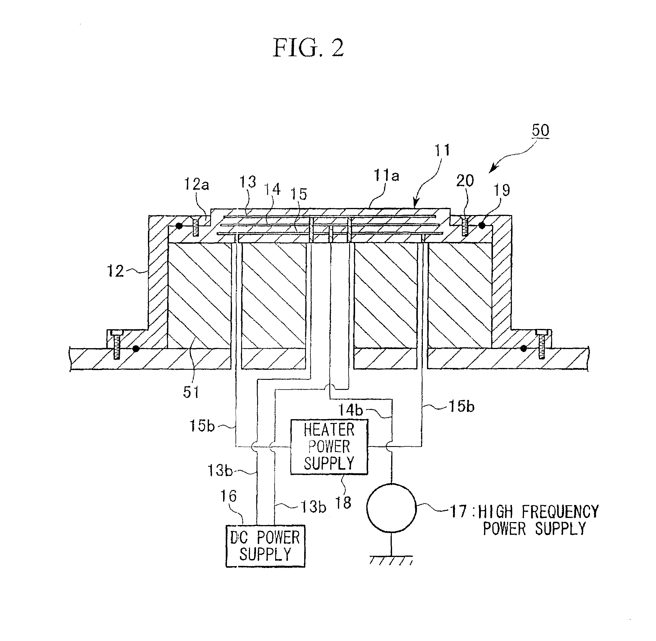
[0073]FIG. 2 is a view showing a second embodiment of a bonding stage that is excellent for implementing the above described flip chip bonding method. In FIG. 2, the descriptor 50 is a bonding stage. The bonding stage 50 differs from the bonding stage 10 shown in FIG. 1 in that a ceramic thermal insulation material 51 is placed in the internal space in the supporting member 12 so as to substantially fill this internal space. Through holes (not shown) that enable the respective wiring 13b, 14b, and 15b connected to the electrodes 13, 14, and 15 to pass through and be guided to the outside are formed in the ceramic thermal insulation material 51.
[0074]The material used for the ceramic thermal insulation material 51 is not particularly restricted; however it is preferable that it be an Al2O3—SiO2—CaO—Li2O based ceramic thermal insulation material. If this type of thermal insulation material is employed, because the ceramic has excellent resistance to compression and ...
examples
[0088]A semiconductor chip packaging test (i.e., a flip chip connection test) was performed using the flip chip bonding method of the present invention, and using the semiconductor chip packaging apparatus 70 shown in FIG. 3. The bumps that were used were composed of Pb / Sn in ratios of 90% by weight to 10% by weight, respectively. The semiconductor test chips used had bump pitches of 200 μm, 150 μm, and 100 μm, and the total number of bumps was 200.
[0089]Prior to the flip chip connection, a circuit substrate on which substrate pad metal and bumps were formed and a semiconductor chip on which chip pad metal was formed were exposed to an Ar plasma atmosphere for one minute. Electricity was then supplied to the heater electrode inside the bonding stage and the heater electrode inside the bonding tool so that the respective temperatures thereof were held at 200° C.
[0090]As a result of performing a flip chip connection in this manner, 100% excellent connections were obtained for each one...
PUM
| Property | Measurement | Unit |
|---|---|---|
| Temperature | aaaaa | aaaaa |
| Pressure | aaaaa | aaaaa |
| Adhesion strength | aaaaa | aaaaa |
Abstract
Description
Claims
Application Information