Fine-pitch packaging substrate and a method of forming the same

Inactive Publication Date: 2005-11-24
VIA TECH INC
View PDF10 Cites 15 Cited by
  • Summary
  • Abstract
  • Description
  • Claims
  • Application Information

AI Technical Summary

Benefits of technology

[0010] The present invention provides a fine-pitch packaging substrate with bonding pads of reduc

Problems solved by technology

However, the density of I/O contacts formed on the packaging substrate is limited by the poor cleanness in packaging process; i.e., the packaging substrate must be lay with a bigger line width with respect to the line width on the die, and so the density of I/O contacts on the packaging substrate is limited thereby.
Basically, when a die is placed on the packaging substrate, an aligning error in between is u

Method used


Image

  • Fine-pitch packaging substrate and a method of forming the same
  • Fine-pitch packaging substrate and a method of forming the same
  • Fine-pitch packaging substrate and a method of forming the same

Examples


Embodiment Construction

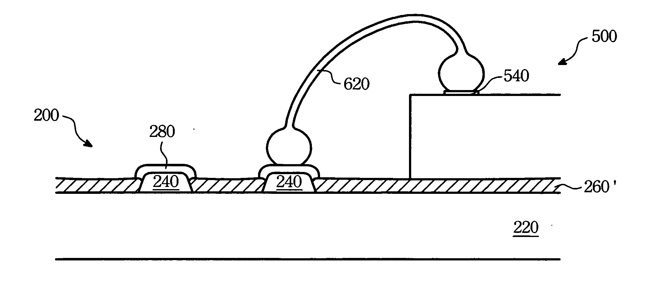
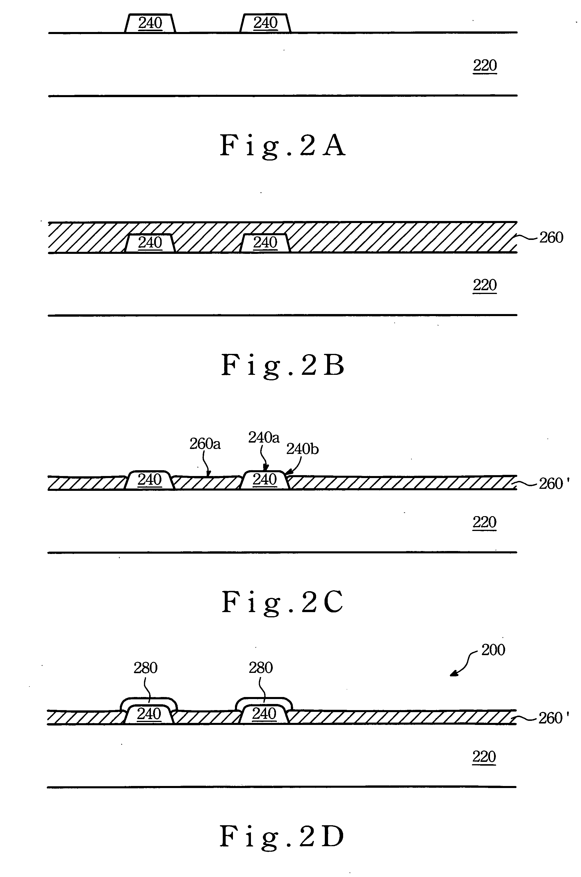
[0021]FIGS. 2A to 2E depict a first preferred embodiment of a packaging method in accordance with the present invention. Firstly, as shown in FIG. 2A, a plurality of bonding pads 240 is formed on an upper surface of a circuit board 220. Afterward, as shown in FIG. 2B, an isolation layer 260 is formed on the circuit board 220 to fill the space between neighboring bonding pads 240 and also cover all the bonding pads 240 and the exposed surfaces of the circuit board 220. Then, referring to FIG. 2C, the isolation layer 260 is partly removed by etching to expose an upper surface 240a and a portion of the sidewall 240b of the bonding pads 240 to conclude an isolation pattern 260′. As a preferred embodiment, the etching process of FIG. 2C may be applied by utilizing a chosen etching solution and a controlled etching duration to adjust the depth of etching to a preset level and have the upper surface 260a of isolation pattern 260 lie at the same level with or below the upper surface 240a of...


PUM


Abstract

A packaging substrate used in a fine-pitch packaging comprises a circuit board, a plurality of packaging pads, an isolation pattern, and a conductive plating layer. The bonding pads are formed on an upper surface of the circuit board for electrically connecting to respective die pads. The isolation pattern filling the space between the neighboring bonding pads can cover all the exposed surfaces of the circuit board. A portion of the isolation pattern adjacent to the bonding pads has a same or a smaller thickness with respect to the bonding pads, and an upper surface and a portion of the sidewall of the packaging pads are thus exposed. The conductive plating layer covering the upper surface and the exposed sidewall of the packaging pads can extend outward from the sidewall to result an increased connectable area.

Description

BACKGROUND OF THE INVENTION [0001] (1) Field of the Invention [0002] This invention relates to a fine-pitch packaging substrate and a method of forming the same, and more particularly to a packaging substrate with a high-density pad array and a method of forming the same. [0003] (2) Description of Related Art [0004] As the prosperity of the semiconductor fabrication technology, a central processing unit (CPU) characterized in small-size, multi-function, and high-speed becomes popular. Such a CPU needs an increased number of input / output (I / O) contacts to transmit data and signals for various functional demands. Thus, the density of I / O contacts must be increased to prevent an increasing packaging size. However, the density of I / O contacts formed on the packaging substrate is limited by the poor cleanness in packaging process; i.e., the packaging substrate must be lay with a bigger line width with respect to the line width on the die, and so the density of I / O contacts on the packagi...

Claims


Application Information

Patent Timeline
IPC IPC(8): H01L21/44H01L21/60H01L23/48H01L23/498H01L23/522H05K1/11H05K3/00H05K3/24H05K3/28
CPCH01L23/49816H01L2224/0401H01L24/81H01L24/85H01L2224/05599H01L2224/48091H01L2224/48227H01L2224/48228H01L2224/48464H01L2224/81801H01L2224/85399H01L2924/01005H01L2924/01006H01L2924/01015H01L2924/01074H01L2924/01075H01L2924/01078H01L2924/014H05K1/111H05K3/002H05K3/243H05K3/28H05K2201/09881H05K2201/10689H05K2203/049H05K2203/0594H01L24/48H01L2224/81136H01L2224/16237H01L2924/01033H01L2924/00014H01L2224/78H01L2224/45099H01L2924/12042H01L2924/00
Inventor HO, KWUN-YAOKUNG, MORISS
Owner VIA TECH INC
Why Eureka
Try Eureka