Apparatus for electroless deposition of metals onto semiconductor substrates

a technology of electroless deposition and semiconductor substrate, which is applied in the direction of spraying apparatus, liquid/solution decomposition chemical coating, coating, etc., can solve the problems of poor substrate temperature control of conventional electroless processing systems and methods, inability to reliably fill interconnect features, and inability to reliably deposition interconnect features, etc., to achieve efficient deposition of conductive layers and minimal defects

Inactive Publication Date: 2005-12-01
APPLIED MATERIALS INC
View PDF99 Cites 67 Cited by
  • Summary
  • Abstract
  • Description
  • Claims
  • Application Information

AI Technical Summary

Benefits of technology

[0010] Embodiments of the invention also provide an electroless deposition system configured to efficiently deposit conductive layers onto semiconductor substrates with minimal defects. The system includes an electroless deposition enclosure positioned on a processing mainframe. The deposition enclosure interior environment is pressure and temperature controlled and inclu...

Problems solved by technology

At these dimensions, conventional deposition techniques, such as chemical vapor deposition and physical vapor deposition, are not able to reliably fill interconnect features.
However, with regard to electroless plating processes, conventional electroless processing systems and methods have faced several challenges, such as accurately controlling the deposition process and the defect ratios in the resulting deposition layers.
More particularly, conventional systems have suffered from poor substrate temperature control, as the resistive heaters and heat lamps used on conven...

Method used


Image

  • Apparatus for electroless deposition of metals onto semiconductor substrates
  • Apparatus for electroless deposition of metals onto semiconductor substrates
  • Apparatus for electroless deposition of metals onto semiconductor substrates

Examples


Embodiment Construction

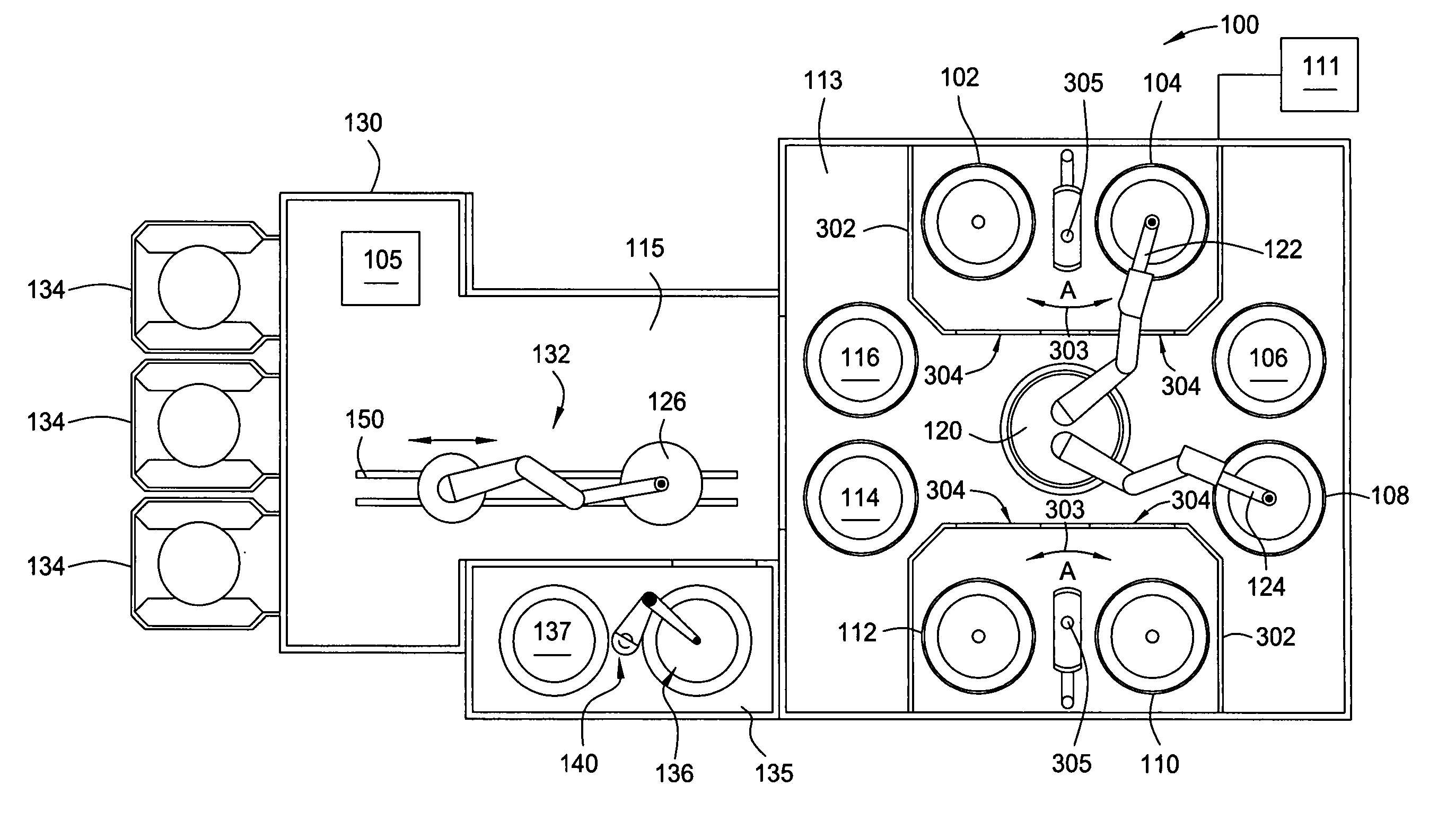
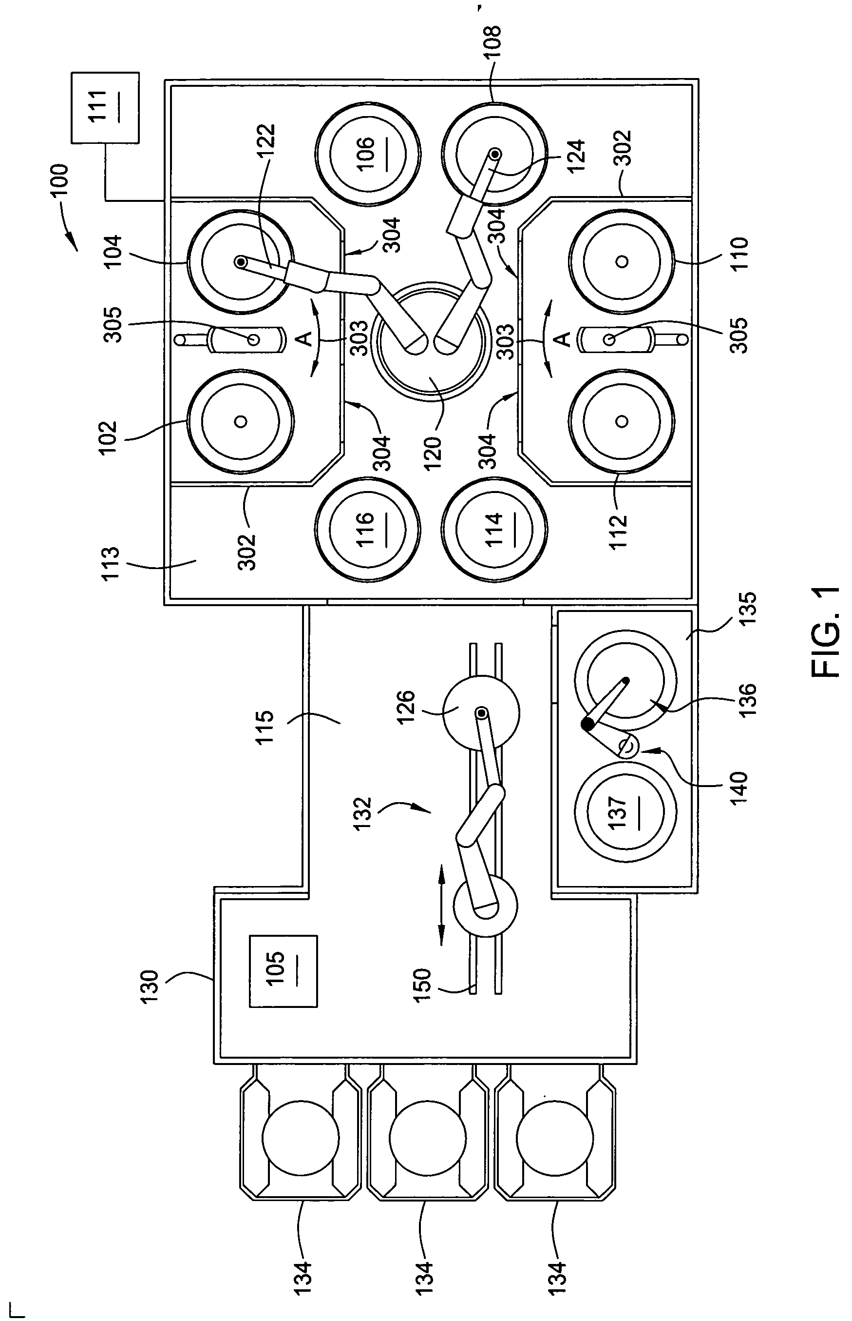
[0029]FIG. 1 illustrates an embodiment of an electroless deposition system 100. System 100 includes a factory interface 130 that includes a plurality of substrate loading stations 134 configured to interface with substrate containing cassettes. A factory interface robot 132 is positioned in the factory interface 130 and is configured to access and transfer substrates 126 into and out of the cassettes positioned on the loading stations 134. The robot 132 also extends into a link tunnel 115 that connects the factory interface 130 to a processing mainframe 113. The position of robot 132 allows for access to loading stations 134 to retrieve substrates therefrom, and to then deliver the substrates 126 to one of the processing cell locations 114, 116 positioned on the mainframe 113, or alternatively, to the annealing station 135. Similarly, robot 132 may be used to retrieve a substrate 126 from the processing cell locations 114, 116 or the annealing station 135 after a substrate processin...


PUM

PropertyMeasurementUnit
Pore sizeaaaaaaaaaa
Pore sizeaaaaaaaaaa
Temperatureaaaaaaaaaa

Abstract

An electroless deposition system is provided. The system includes a processing mainframe, at least one substrate cleaning station positioned on the mainframe, and an electroless deposition station positioned on the mainframe. The electroless deposition station includes an environmentally controlled processing enclosure, a first processing station configured to clean and activate a surface of a substrate, a second processing station configured to electrolessly deposit a layer onto the surface of the substrate, and a substrate transfer shuttle positioned to transfer substrates between the first and second processing stations. The system also includes a substrate transfer robot positioned on the mainframe and configured to access an interior of the processing enclosure. The system also includes a substrate a fluid delivery system that is configured to deliver a processing fluid by use of a spraying process to a substrate mounted in the processing enclosure.

Description

CROSS-REFERENCE TO RELATED APPLICATIONS [0001] This application claims benefit of U.S. Provisional Patent Application Ser. No. 60 / 539,491, titled “Apparatus for Electroless Deposition of Metals onto Semiconductor Wafers,” filed Jan. 26, 2004, and U.S. Provisional Patent Application Ser. No. 60 / 575,553, titled “Face Up Electroless Plating Cell,” filed May 28, 2004, and is a continuation-in-part of U.S. patent application Ser. No. 10 / 996,342, titled “Apparatus for Electroless Deposition of Metals onto Semiconductor Substrates,” filed Nov. 22, 2004, which also claims the benefit of the filing dates of the 60 / 539,491 and 60 / 575,553 provisional applications, all of which are incorporated herein by reference.BACKGROUND OF THE INVENTION [0002] 1. Field of the Invention [0003] Embodiments of the invention generally relate to an electroless deposition system for semiconductor processing. [0004] 2. Description of the Related Art [0005] Metallization of sub 100 nanometer sized features is a fo...

Claims


Application Information

Patent Timeline
IPC IPC(8): B05D3/10C23C18/16C23F1/00H01L21/00H01L21/306
CPCC23C18/1628H01L21/67155H01L21/6723H01L21/6719H01L21/67167
Inventor LUBOMIRSKY, DMITRYSHANMUGASUNDRAM, ARULKUMARELLWANGER, RUSSELLPANCHAM, IAN A.CHEBOLI, RAMAKRISHNAWEIDMAN, TIMOTHY W.
Owner APPLIED MATERIALS INC
Why Eureka
Try Eureka