Check patentability & draft patents in minutes with Patsnap Eureka AI!

Circuit board assembly employing solder vent hole

a technology of circuit board and solder vent hole, which is applied in the direction of printed circuit, printed circuit components, printed circuit manufacturing, etc., can solve the problem of no intimate metal-to-metal contact between metal substrates, and achieve the effect of relieving pressure in the cavity

Inactive Publication Date: 2005-12-01
INTEL CORP
View PDF7 Cites 4 Cited by
  • Summary
  • Abstract
  • Description
  • Claims
  • Application Information

AI Technical Summary

Benefits of technology

This approach enables cost-effective nonconductive adhesive bonding with effective electrical and thermal coupling, ensuring reliable grounding and heat dissipation for high power electronics assemblies.

Problems solved by technology

The drawback to this approach is that there is no intimate metal-to-metal contact between the metal substrate and the metalized backside of the PCB.
However, trapped air and gases created during the solder reflow process create backpressure and prevent the molten solder from flowing.

Method used


Image

  • Circuit board assembly employing solder vent hole
  • Circuit board assembly employing solder vent hole
  • Circuit board assembly employing solder vent hole

Examples


Embodiment Construction

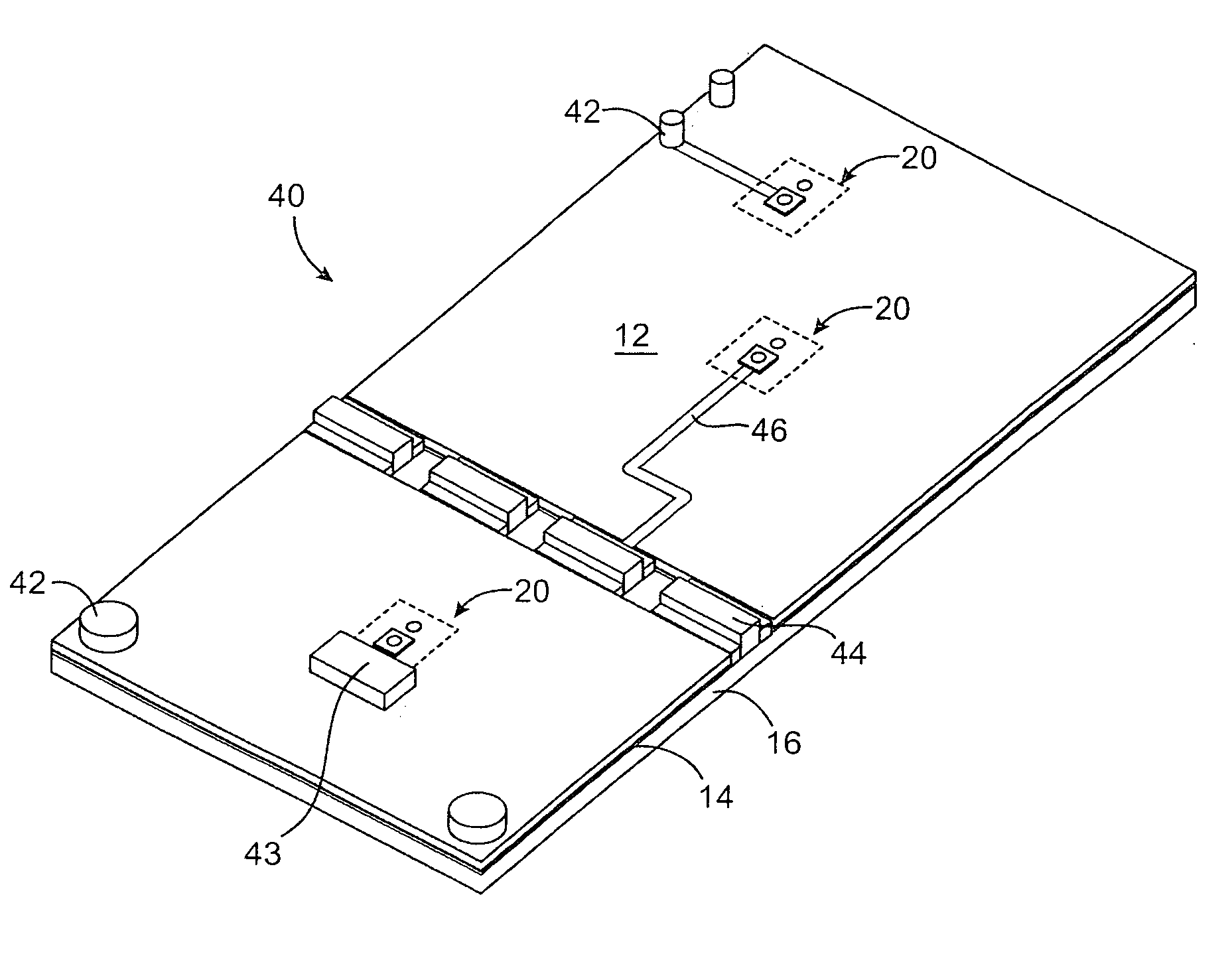
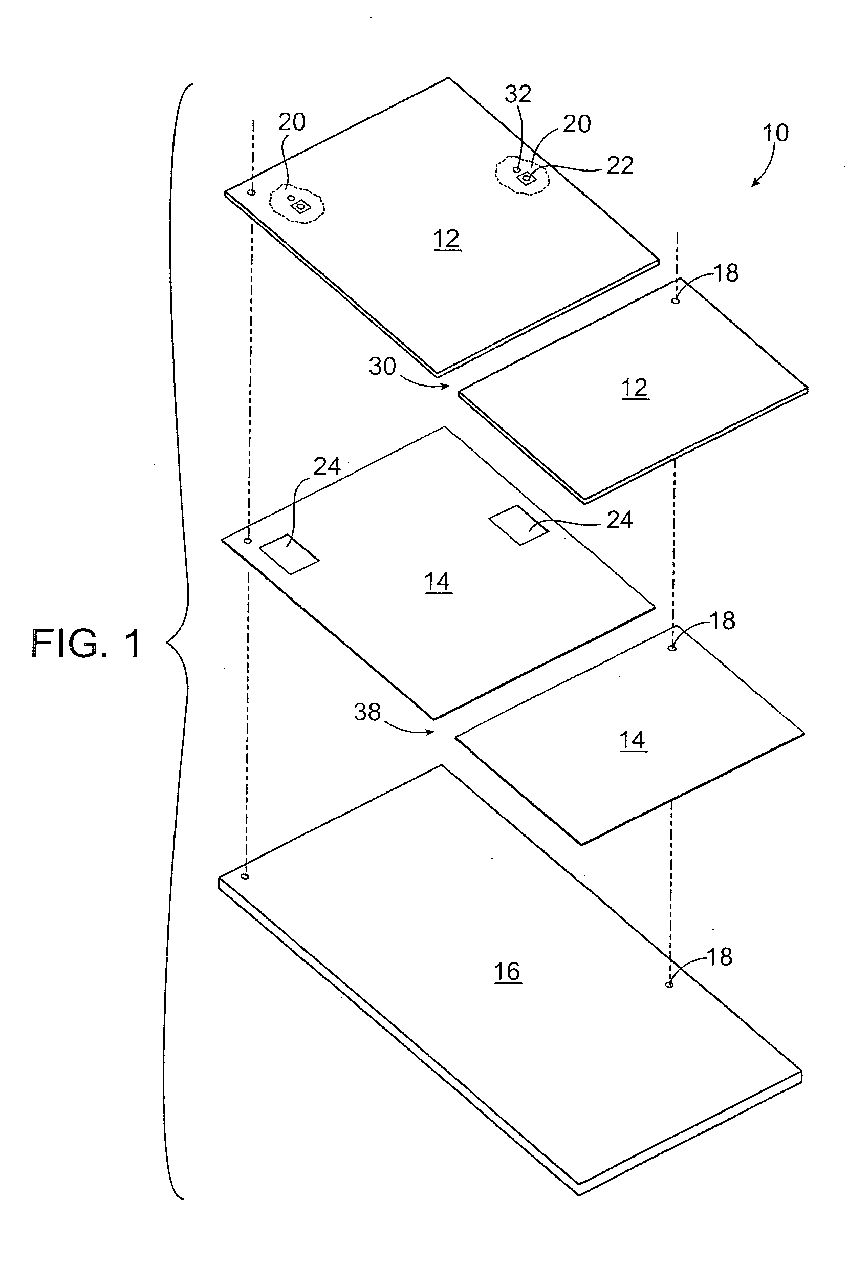
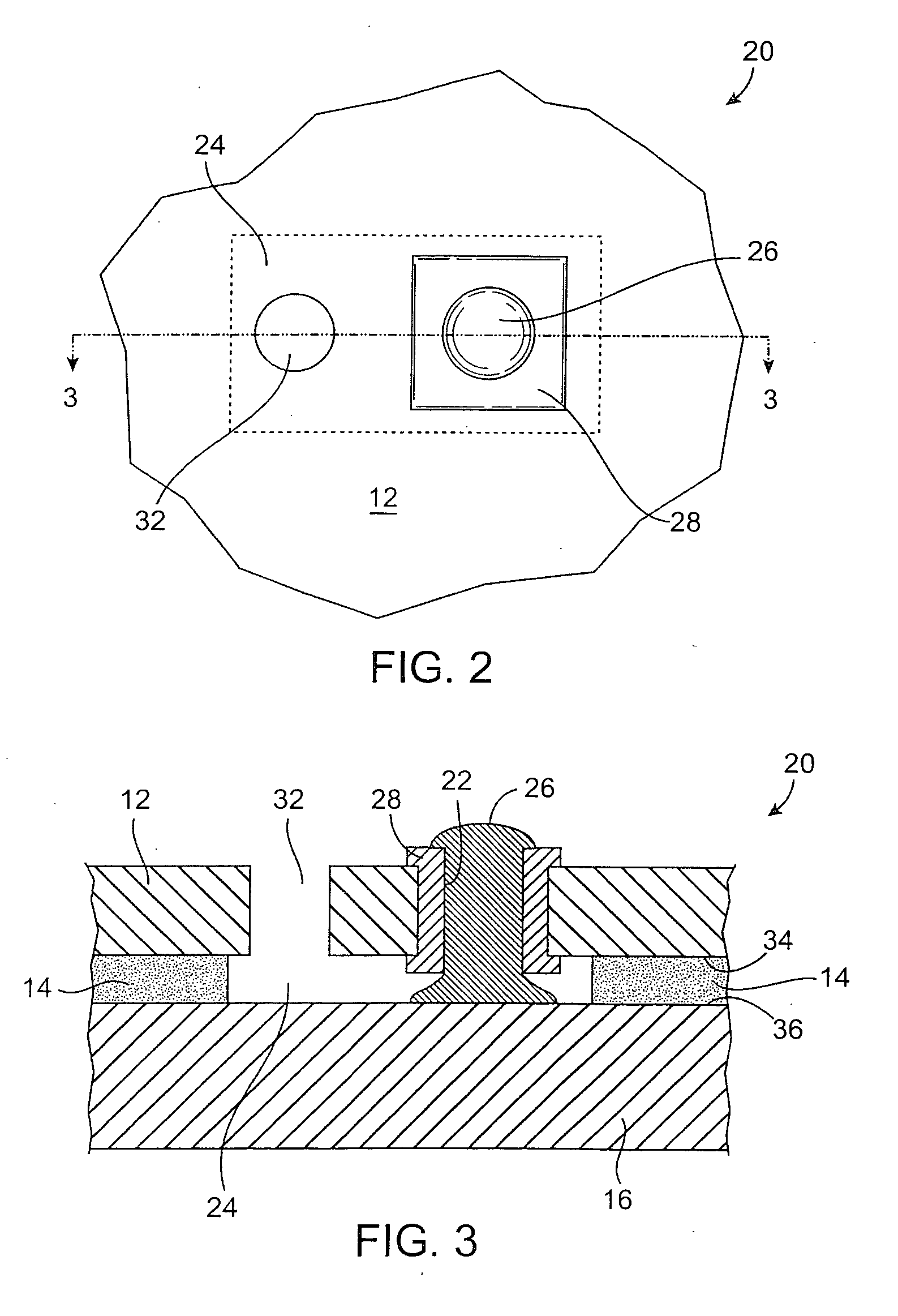
[0020]FIG. 1 is an exploded perspective view of an electronics assembly 10 in accordance with a preferred embodiment of the present invention. In this example, assembly 10 comprises printed circuit board (PCB) layer 12, nonconductive adhesive layer 14, and a conductive support substrate or pallet 16. Pallet 16 is composed of a good electrical and thermal conductor, preferably a metal such as copper. Printed circuit board layer 12 is attached to the conductive substrate 16 using the nonconductive adhesive 14 (as shown in FIG. 3). For example, a thermal set sheet epoxy 14 may be employed. The use of a thermal set nonconductive adhesive sheet (or preform) to attach a printed circuit board to a metal substrate is disclosed in U.S. Pat. No. 6,421,253 to Daniel Ash, Jr., issued Jul. 16, 2002, the disclosure of which is incorporated herein by reference in its entirety. The PCB layer 12 includes various active and passive electronic components (shown generally in FIG. 4) and in one preferre...


PUM

PropertyMeasurementUnit
conductiveaaaaaaaaaa
electrically conductiveaaaaaaaaaa
thermally conductiveaaaaaaaaaa

Abstract

A printed circuit board assembly employing a solder vent hole adjacent solder filled interconnect vias connecting to a conductive pallet, is disclosed. The solder vent hole allows gases to escape from an otherwise sealed cavity during solder reflow, relieving positive pressure and thereby allowing solder to flow into it. By providing an escape path for trapped air and gases generated during solder paste reflow, the out-gassing pressure and weight of the molten solder is sufficient to allow the solder paste to flow into the cavity.

Description

RELATED APPLICATION INFORMATION [0001] This patent application claims the benefit pursuant to 35 USC §119(e) of the priority date of U.S. Provisional Patent Application Ser. No. 60 / 472,710, filed on May 22, 2003, the entire contents of which are hereby expressly incorporated herein by reference.BACKGROUND OF THE INVENTION [0002] 1. Field of the Invention [0003] The present invention relates to printed circuit board assemblies and methods for assembling electronic components into multi-layer assemblies. More particularly, the present invention relates to RF power amplifier circuit board assemblies and related methods of assembly. [0004] 2. Description of the Prior Art and Related Background Information [0005] In high power electronics assemblies generating a relatively high amount of heat, it is typically necessary to attach a printed circuit board (PCB) containing electronic components to a metal substrate provided as a heat sink. RF power amplifiers are an example of such electroni...

Claims


Application Information

Patent Timeline
Patent Type & Authority Applications(United States)
IPC IPC(8): H05K3/00H05K3/34H05K3/44
CPCH05K3/0061H05K3/341H05K3/44H05K2201/09063H05K2201/09554Y10T29/49155H05K2203/1178Y10T29/49144Y10T29/49126Y10T29/49165H05K2201/10666Y02P70/50H05K3/34
Inventor WONG, KENNETH DARYLBELL, SEAN L.
Owner INTEL CORP
Features
  • R&D
  • Intellectual Property
  • Life Sciences
  • Materials
  • Tech Scout
  • Unparalleled Data Quality
  • Higher Quality Content
  • 60% Fewer Hallucinations
Learn More