Metal-insulator-metal capacitor having a large capacitance and method of manufacturing the same

a technology of metal-insulator and capacitor, which is applied in the field of analogue mim capacitor, can solve the problems of limiting the thickness of the dielectric film of the above-described mim capacitor, affecting the fabrication of high-speed capacitors with a large capacitance, and restricting the increase of the capacitance of the above conventional mim capacitor, so as to achieve a large capacitance, prevent a leakage current, and increase the capacitance of the mim capacitor

Inactive Publication Date: 2005-12-01
SAMSUNG ELECTRONICS CO LTD
View PDF10 Cites 28 Cited by
  • Summary
  • Abstract
  • Description
  • Claims
  • Application Information

AI Technical Summary

Benefits of technology

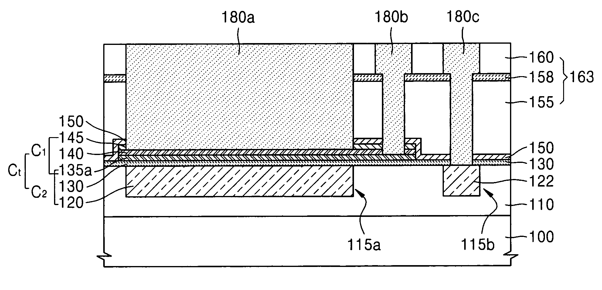
[0014] It is a feature of an embodiment of the present invention to provide a MIM capacitor that is capable of having a large capacitance and preventing a leakage current.
[0015] It is another feature of an embodiment of the present invention to provide a MIM capacitor including at least one capacitor connected in parallel, thereby increasing a capacitance of the MIM capacitor.
[0016] It is still another feature of an embodiment of the present invention to provide a MIM capacitor that is able to increase a capacitance of the capacitor without reducing a thickness of a dielectric film of the capacitor, thereby improving prevention of leakage current.

Problems solved by technology

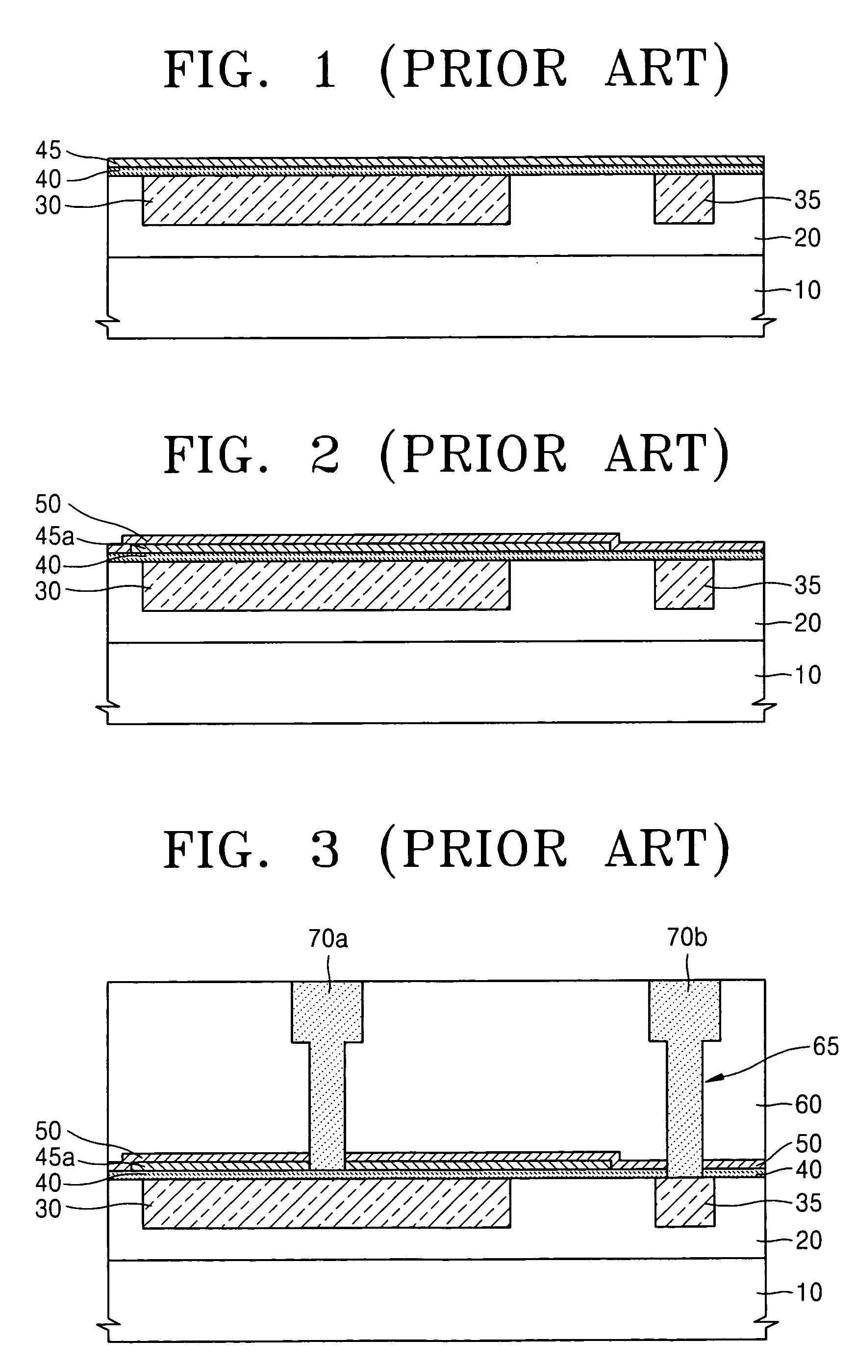
The polysilicon layer, however, has a large resistance and is easily oxidized, which impedes fabrication of a high-speed capacitor having a large capacitance.
However, the above-described MIM capacitor is limited in how much a thickness of the dielectric film may be reduced due to a high possibility of causing a leakage current.
Therefore, an increase in the capacitance of the above conventional MIM capacitor is restricted.
Although a capacitor area can be increased by another method of increasing the capacitance of the MIM capacitor, the above conventional MIM capacitor is also limited in increasing the capacitor area in view of the trend toward integrating the devices.

Method used


Image

  • Metal-insulator-metal capacitor having a large capacitance and method of manufacturing the same
  • Metal-insulator-metal capacitor having a large capacitance and method of manufacturing the same
  • Metal-insulator-metal capacitor having a large capacitance and method of manufacturing the same

Examples


Embodiment Construction

[0040] Korean Patent Application No. 2004-38174, filed on May 28, 2004, in the Korean Intellectual Property Office, and entitled: “Metal-Insulator-Metal Capacitor With High Capacitance and Method of Manufacturing the Same,” is incorporated by reference herein in its entirety.

[0041] The present invention will now be described more fully hereinafter with reference to the accompanying drawings, in which exemplary embodiments of the invention are shown. The invention may, however, be embodied in different forms and should not be construed as limited to the embodiments set forth herein. Rather, these embodiments are provided so that this disclosure will be thorough and complete, and will fully convey the scope of the invention to those skilled in the art. In the figures, the dimensions of films, layers and regions are exaggerated for clarity of illustration. It will also be understood that when a layer is referred to as being “on” another layer or substrate, it can be directly on the ot...


PUM

PropertyMeasurementUnit
lengthaaaaaaaaaa
widthaaaaaaaaaa
depthaaaaaaaaaa

Abstract

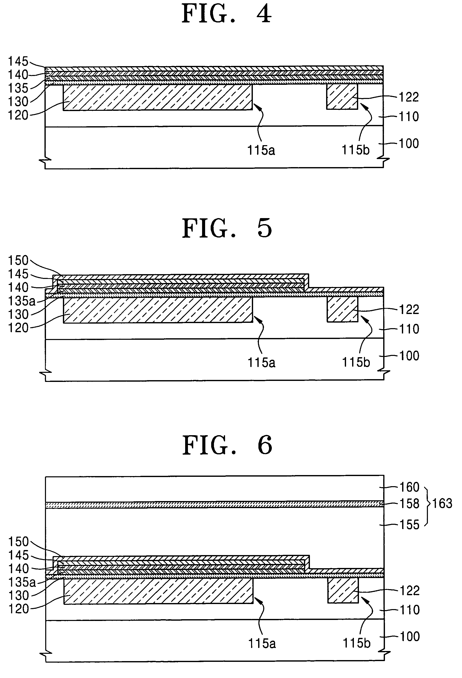
A metal-insulator-metal (MIM) capacitor having a large capacitance, and a method of manufacturing the same, includes forming a lower electrode on a semiconductor substrate, sequentially forming a first dielectric film, an intermediary electrode, and a second dielectric film on an upper surface of the lower electrode, forming an inter-metal insulating layer on an upper surface of the second dielectric film, etching predetermined portions of the inter-metal insulating layer to form an upper electrode region and via hole regions, selectively etching the second dielectric film exposed in a portion of the via hole regions to expose the intermediary electrode, and forming a metal layer on the upper electrode region and the via hole regions, thereby forming an upper electrode and contact plugs.

Description

BACKGROUND OF THE INVENTION [0001] 1. Field of the Invention [0002] The present invention relates to a Metal-Insulator-Metal (MIM) capacitor and a method of manufacturing the same. More particularly, the present invention relates to an analog MIM capacitor having a large capacitance and a method of manufacturing the same. [0003] 2. Description of the Related Art [0004] As semiconductor integrated circuits become more diversely used, an analog capacitor formed in a logic circuit area is required to attain a high speed and a large capacitance. A high-speed capacitor may be achieved by lowering a resistance of a capacitor electrode to decrease reliance on frequency. A large-capacitance capacitor may be achieved by decreasing a thickness of a capacitor dielectric film, using a dielectric film with a high dielectric constant, or increasing a capacitor area. [0005] In such an analog capacitor, an electrode is generally formed of a polysilicon layer. The polysilicon layer, however, has a l...

Claims


Application Information

Patent Timeline
Patent Type & Authority Applications(United States)
IPC IPC(8): H01L27/04H01L21/00H01L21/02H01L21/822H01L27/08H01L29/00
CPCH01L28/60H01L27/0805H01L27/04
Inventor CHO, KWANG-LAE
Owner SAMSUNG ELECTRONICS CO LTD
Why Eureka
Try Eureka