

Method for controlled ink-jet spreading of polymers for the insulation and/or protection of printed circuits
- Summary
- Abstract
- Description
- Claims
- Application Information
AI Technical Summary
Benefits of technology
Problems solved by technology
Method used
Image

Examples
Embodiment Construction
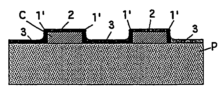
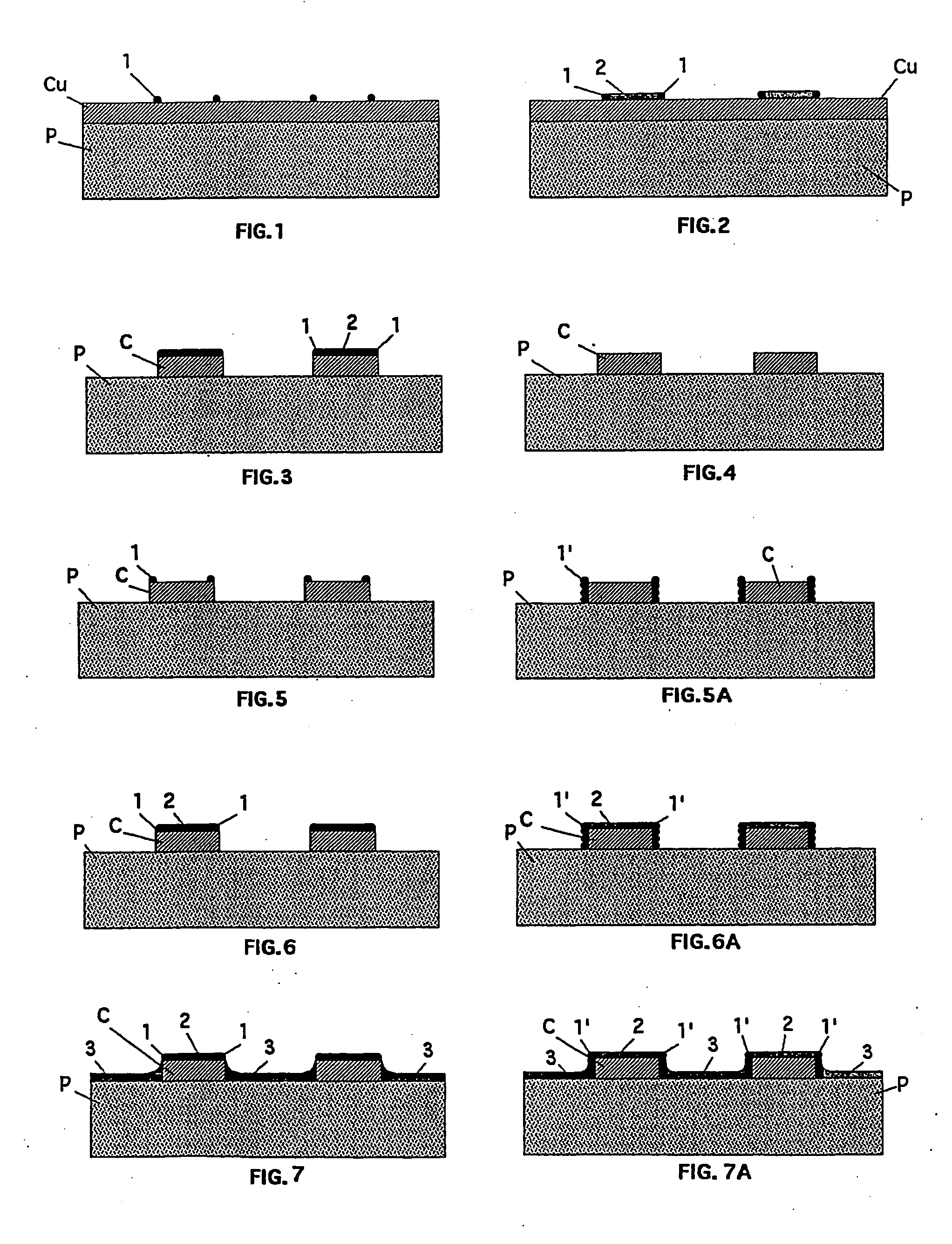
[0027] The invention is now described with the aid of the enclosed drawings that illustrate in a schematic cross section a portion of a printed circuit card in the specific case concerned, in an enlarged view of two electric conductor lines.
[0028] All the deposits are made by means of a pixel jet system namely with the so-called inkjet system where, in contrast, ink is sprayed in pixels (punctiform droplets) onto said insulating polymeric material for protection and / or insulation.
BRIEF DESCRIPTION OF THE DRAWINGS
[0029]FIG. 1 represents the first deposition phase of the edge of the design of the printed board on the copper layer of the card (design border-contour).
[0030]FIG. 2 represents the second filling phase with the protective and insulating material of the printed board design.
[0031]FIG. 3 represents the engraving phase, namely the removal phase of the copper layer not concerning the printed board design, exposing the underlying support material of the card, namely the plas...
PUM
| Property | Measurement | Unit |
|---|---|---|
| Length | aaaaa | aaaaa |
| Length | aaaaa | aaaaa |
| Thickness | aaaaa | aaaaa |
Abstract
Description
Claims
Application Information