Integrating/SAR ADC and method with low integrator swing and low complexity

a technology of integrator swing and integrator, applied in the field of hybrid deltasigma/sar analog to digital converter, can solve the problems of increasing exponentially the number of samples (n) to create a defined output resolution of adc result b>140/b>, and requiring substantial conversion time for relatively high resolution

Active Publication Date: 2009-03-31
TEXAS INSTR INC
View PDF13 Cites 34 Cited by
  • Summary
  • Abstract
  • Description
  • Claims
  • Application Information

AI Technical Summary

Benefits of technology

[0021]It is another object of the invention to provide a circuit and method which provides a hybrid delta-sigma / SAR ADC in which the output voltage swing of an integrator therein is reduced without increasing the amount of integrated circuit chip area required.
[0022]It is another object of the invention to provide a circuit and method which provides a hybrid delta-sigma / SAR ADC in which the output voltage swing of an integrator therein is reduced without increasing the number of integration capacitors or increasing the settling time of the integrator output signal.
[0023]It is another object of the invention to provide a circuit and method which provides a complete, very accurate digital temperature sensor on the smallest practical integrated circuit chip, requiring the smallest practical power supply voltage, and requiring lowest amount of quiescent current.
[0026]In a described embodiment, the digital control circuitry (28) performs a fourth cycle (Cycle1) before the first (Cycle2), second (Cycle3) and third (Cycle4) cycles, the fourth cycle (Cycle1) including integrating a value of the input voltage (ΔVbe) in a second direction by means of the integrator (30) so as to substantially reduce a voltage swing of the output (Vout) of the integrator (30). Each of the plurality of switches (SW1-6) is controlled by the digital control circuitry (28). In a described embodiment, the digital control circuitry (28) executes an algorithm represented by
[0036]In a described embodiment, the input voltage (ΔVbe) is produced by an input circuit (13) including first (MN0) and second (MN1) transistors and first (I0) and second (I1) variable current sources so as to cause the input voltage (ΔVbe) to represent a temperature of the first (MN0) and second (MN1) transistors, the first transistor (MM0) having an emitter connected to a supply voltage (VSS) and a base and collector connected by a first input conductor (11) to the first variable current source (I0), the second transistor (MN1) having an emitter connected to the supply voltage (VSS) and a base and collector connected by a second input conductor (12) to the second variable current source (I1), the input voltage (ΔVbe) being applied between the first (11) and second (12) input conductors. The digital circuitry (28) controls values of currents produced by the first (I0) and second (I1) variable current sources, respectively, so as to establish a desired amplitude of the separate voltage (Vbe) and a desired amplitude and polarity of the input voltage (ΔVbe). The algorithm limits and amplitude of the output voltage (Vout) produced by the integrator (30) to thereby allow accurate operation of the reconfigurable circuitry (10) with a low power supply voltage.
[0037]In one embodiment, the invention provides a method of operating reconfigurable circuitry (10) in a hybrid delta-sigma / SAR ADC (analog-to-digital converter)(400), the reconfigurable circuitry (10) including an integrator (30) including an amplifier (15), a plurality of input capacitors (C0,1,2,3,6,7), first (C4) and second (C5) integrating capacitors, a plurality of switches (SW1-6) for selectively coupling the plurality of input capacitors (C0,1,2,3,6,7) and the first (C4) and second (C5) integrating capacitors to various terminals of the amplifier (15) and input terminals (11,12) of the integrator (30) to effectuate operation of the hybrid delta-sigma / SAR ADC (400) in delta-sigma ADC and SAR ADC modes thereof, and a comparator (22) coupled to an output voltage (Vout) of the integrator (30), the method including controlling the plurality of switches (SW1-6) by performing a plurality of cycles (Cycles2,3,4) of SAR operation of the hybrid delta-sigma / SAR ADC (400) for generating one SAR bit or each of a plurality of SAR bits, the controlling in effect creating an entire reference voltage value (Vref) equal to the sum of a first voltage (ΔVbe) of the integrator (30) and a second voltage (Vbe), performing a first cycle (Cycle2) by multiplying a residue voltage (Vresidue) of the integrator (30) by 2, performing a second cycle (Cycle3) by integrating the second voltage (Vbe) in a first direction by means of the integrator (30) if the comparator (22) changes state or in a second direction opposite to the first direction if the comparator (22) does not change state, and performing a third cycle (Cycle4) by integrating the first voltage (ΔVbe) in a direction that causes the output voltage (Vout) of the integrator (30) to equal either 2×Vresidue−Vref or 2×Vresidue+Vref, wherein Vresidue is a residue voltage which is an output voltage of the integrator (30) at the end of a preceding cycle and Vref is equal to the entire reference voltage value (ΔVbe+Vbe). In one embodiment the first voltage is an input voltage (ΔVbe) of the hybrid delta-sigma / SAR ADC (400). In one embodiment, the method includes performing a fourth cycle (Cycle1) before the first (Cycle2), second (Cycle3) and third (Cycle4) cycles, the fourth cycle (Cycle1) including integrating a value of the input voltage (ΔVbe) in a second direction by means of the integrator (30) so as to substantially reduce a voltage swing of the output voltage (Vout) of the integrator (30).

Problems solved by technology

The number of iterations typically affects the noise level of any result as well as the resolution of the ultimate digital signal.
Unfortunately, the number of samples (N) to create a defined output resolution of ADC result 140 increases exponentially.
Thus, while analog to digital converter 100 is capable of providing accurate results, results exhibiting relatively high resolution require substantial conversion time.
However, while analog to digital converter 170 is capable of providing quick results, the results are often inaccurate due to noise.
At high operating temperatures, the previously mentioned “leaky” low voltage integrated circuit manufacturing processes result in relatively high leakage currents.
This is a serious limitation for the accuracy of an ADC manufactured using such processes.
It requires more complicated switches as additional switching modes are introduced.
Unfortunately, mixed or hybrid delta-sigma / SAR ADC architectures require more complex switching than ADCs including only delta-sigma architecture or including only SAR architecture.
A serious problem of the hybrid delta-sigma / SAR ADC as described in above mentioned commonly assigned patent application Ser. No. 11 / 738,566 is the amount of output voltage swing required at the output of the integrator when the hybrid delta-sigma / SAR is operating in its SAR mode.
The necessary output voltage swing results in an undesirable limitation on the minimum power supply voltage at which the hybrid delta-sigma / SAR can operate.
The necessary output voltage swing can be reduced by increasing the number of integration capacitors, but that has the undesired effect of increasing the amount of required integrated circuit chip area and either increasing the quiescent current required in the integrator or having an accordingly longer settling time needed every half cycle for the integrator output voltage to settle to the necessary value with the necessary accuracy.

Method used


Image

  • Integrating/SAR ADC and method with low integrator swing and low complexity
  • Integrating/SAR ADC and method with low integrator swing and low complexity
  • Integrating/SAR ADC and method with low integrator swing and low complexity

Examples


Embodiment Construction

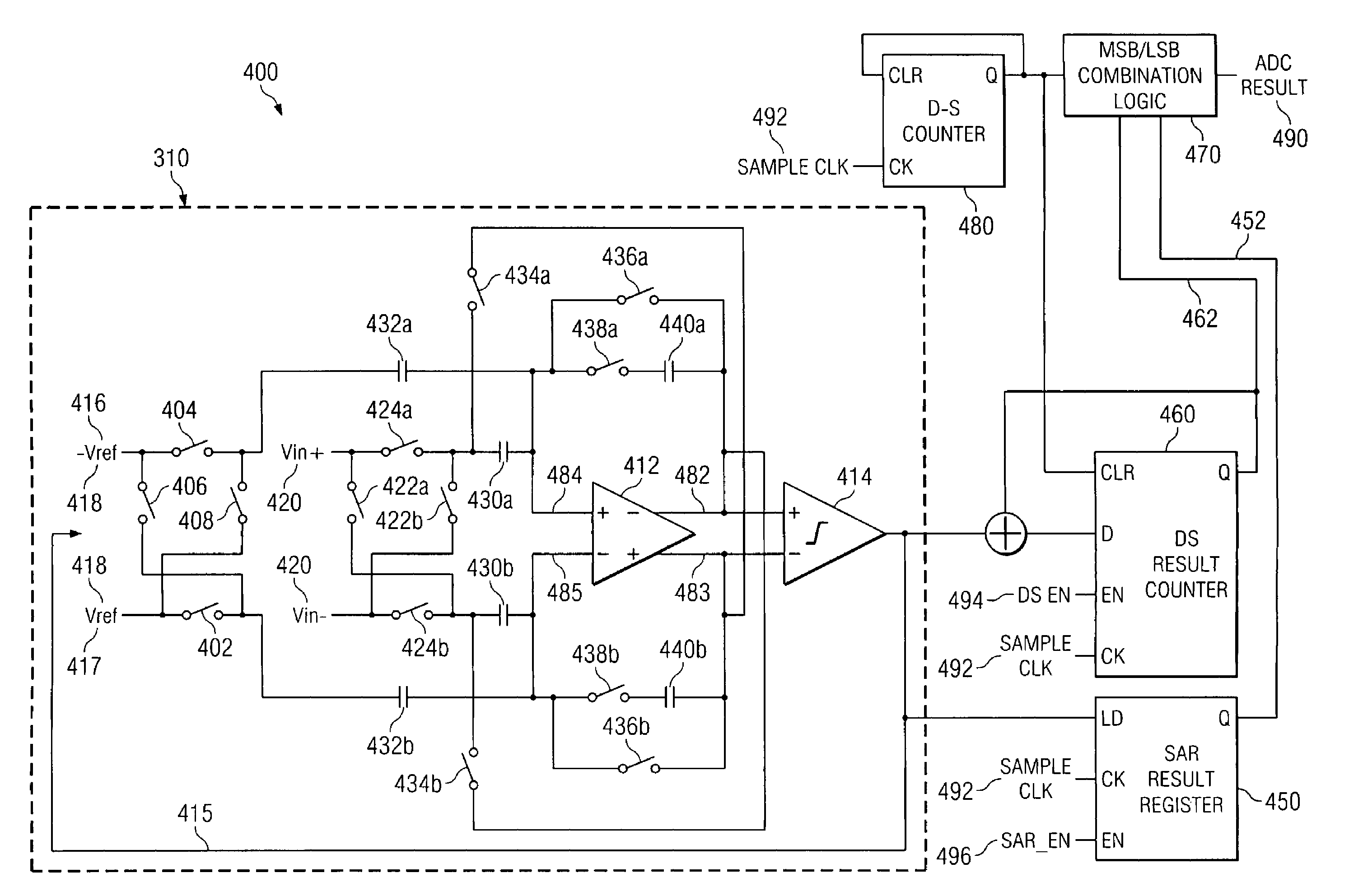
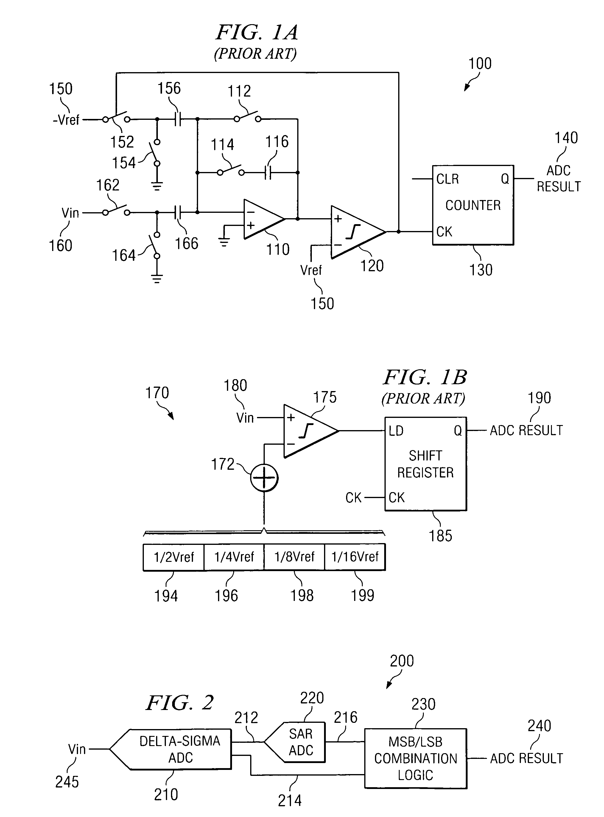
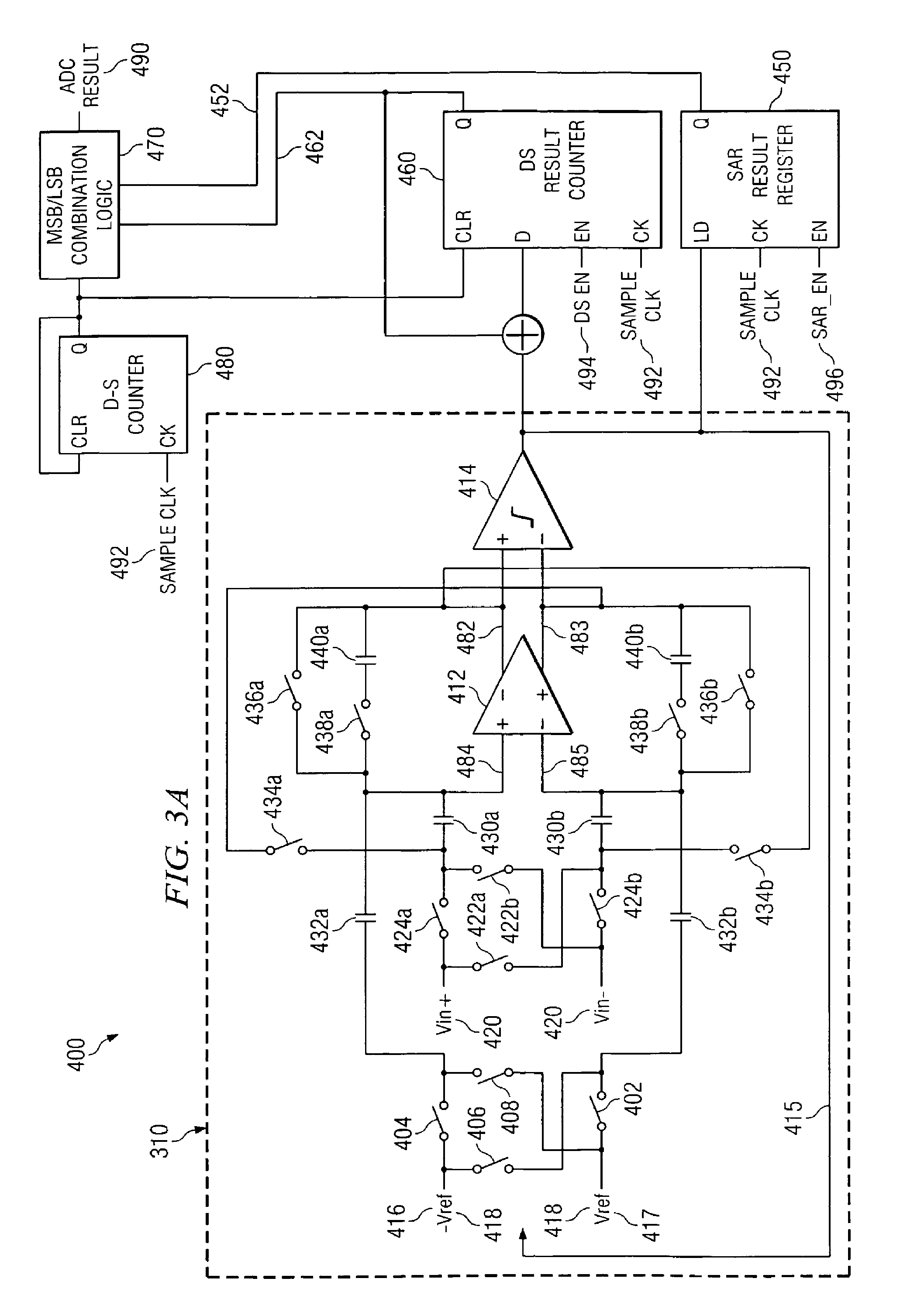
[0048]Referring to FIG. 2, a combined delta-sigma and SAR (i.e., “Successive Approximation Register”) based analog to digital converter (ADC) 200 in accordance with various embodiments of the present invention is depicted. Analog to digital converter 200 includes a first stage delta-sigma analog to digital converter 210, a second stage SAR analog to digital converter 220, and a combination block 230. Delta-sigma analog to digital converter 210 receives a voltage input 245 that is to be sampled. Delta-sigma analog to digital converter 210 performs a delta-sigma based analog to digital conversion that provides a first portion of a conversion result 214 and a conversion residue 212. The first portion of the conversion result 214 and conversion residue 212 are formed using delta-sigma conversion techniques that are more fully discussed below in relation to FIG. 3B. Further, it should be noted that delta-sigma analog to digital converter 210 may be implemented as any of a variety of circ...


PUM


Abstract

A reconfigurable circuit (10) includes an integrator (30) having switches (SW1-6) for selectively coupling input capacitors (C0,1,2,3,6,7) and integrating capacitors (C4,5) to terminals of the integrator (30) for operation of a hybrid delta-sigma / SAR ADC (400) so as to create a reference voltage value (Vref) equal to the sum of a first voltage (ΔVbe) and a second voltage (Vbe). A first integration is performed to reduce the integrator output voltage swing. A residue (Vresidue) of the integrator is multiplied by 2. Then the second voltage (Vbe) is integrated in a first direction if a comparator (22) coupled to the integrator changes state or in an opposite direction if the comparator does not change state. The first voltage (ΔVbe) is integrated in a direction that causes the integrator output voltage (Vout) to equal either 2×Vresidue−Vref or 2×Vresidue+Vref.

Description

CROSS REFERENCE TO RELATED APPLICATION[0001]This application is a continuation-in-part of commonly assigned patent application Ser. No. 11 / 738,566 entitled “Hybrid Delta-Sigma / SAR Analog to Digital Converter and Methods for Using Such”, filed Apr. 23, 2007 by Jerry Doorenbos, Marco Gardner and Dimitar Trifonov, and incorporated herein by reference.BACKGROUND OF THE INVENTION[0002]The present invention relates generally to hybrid delta-sigma / SAR analog to digital converters (ADCs) of the type described in above-mentioned commonly assigned patent application Ser. No. 11 / 738,566. More particularly, the present invention relates to improvements which provide minimum integrator output swing, operation with very low power supply voltage, reduced quiescent current, and high accuracy even though the integrated circuit hybrid delta-sigma / SAR ADC is fabricated using low voltage “leaky” manufacturing processes.[0003]Various analog to digital data converters and conversion techniques have been ...

Claims


Application Information

Patent Timeline
Patent Type & Authority Patents(United States)
IPC IPC(8): H03M3/00
CPCH03M1/145H03M1/46H03M3/46
Inventor TRIFONOV, DIMITAR T.DOORENBOS, JERRY L.
Owner TEXAS INSTR INC
Why Eureka
Try Eureka