Nitride semiconductor laser device

a laser device and nitride technology, applied in the direction of semiconductor laser structure details, semiconductor lasers, optical resonator shape and construction, etc., can solve the problems of shortening the lifetime and deteriorating the output light intensity so as to prevent the blackening of the resonator end surface, shorten the lifetime of the nitride semiconductor laser element, and prevent the effect of deterioration in output light intensity

Active Publication Date: 2005-12-01
SHARP FUKUYAMA LASER CO LTD
View PDF5 Cites 17 Cited by
  • Summary
  • Abstract
  • Description
  • Claims
  • Application Information

AI Technical Summary

Benefits of technology

[0009] The present invention has been made for solving the above-described problem of the conventional art and an object of the present invention is to provide a nitride semiconductor laser device, preventing blackening of a resonator end surface of a nitride semiconductor laser element and thereby preventing deterioration in output light intensity or shortening of the lifetime of the nitride semiconductor laser element that is caused by the blackening.

Problems solved by technology

The blackening results in a problem of deterioration in output light intensity of the nitride semiconductor laser element or shortening of the lifetime thereof.

Method used


Image

  • Nitride semiconductor laser device
  • Nitride semiconductor laser device
  • Nitride semiconductor laser device

Examples


example 1

[0067] As a nitride semiconductor laser element, a semiconductor laser of InGaN having an output wavelength of 410 nm was used to produce a nitride semiconductor laser device as shown in FIG. 1. At this time, the dew point and the oxygen concentration of the enclosed atmosphere were set respectively at −40° C. and 100 ppm. Further, as an enclosed gas, nitrogen was supplied at a pressure of 102660 Pa.

[0068] Under the above-described conditions, the ratio of blackened elements was measured. The ratio was approximately 20% or less.

[0069] For comparison with the arrangement as shown in FIG. 1 that has the light detecting element enclosed within the cap, an arrangement having the light detecting element outside the nitride semiconductor laser device was examined. It was found that, on a surface of the light detecting element where intense light emitted from the nitride semiconductor laser device is concentrated, blurring of the surface occurred. The blurring of the surface of the light...

example 2

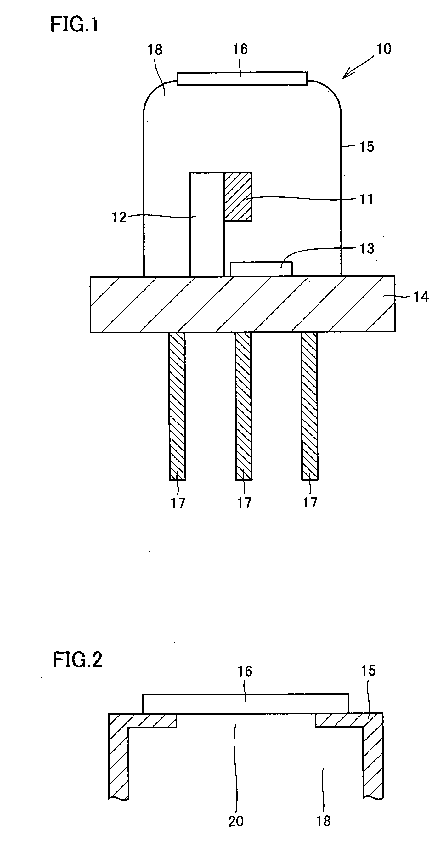
[0072] A nitride semiconductor laser device of Example 2 differs from that of Example 1 (FIG. 1) in that heat sink 12 and stem 14 are integrated into one component or stem 14 has a protrusion that supports a nitride semiconductor laser element as shown in FIG. 5. Other structural features as well as the effects derived therefrom are similar to those as shown in FIG. 1.

[0073] When the heat sink and the stem are provided as an integrated component or the stem has the protrusion supporting the nitride semiconductor laser element (hereinafter referred to as integrated stem), because of the fact that the heat sink portion and the stem portion are constituted of the same material, the heat sink portion and the stem portion and respective functions cannot be distinguished from each other, as shown in FIG. 5. Thus, heat sink 12 and stem 14 are not regarded as separate components as shown in FIG. 1. Instead, the heat sink and the stem may be regarded as a single stem 14 as shown in FIG. 5. ...

example 3

[0077] A nitride semiconductor laser device of Example 3 differs from that of Example 1 (FIG. 1) in that no light detecting element is provided. Other structural features as well as the effects derived therefrom are similar to those of Example 1 or Example 2.

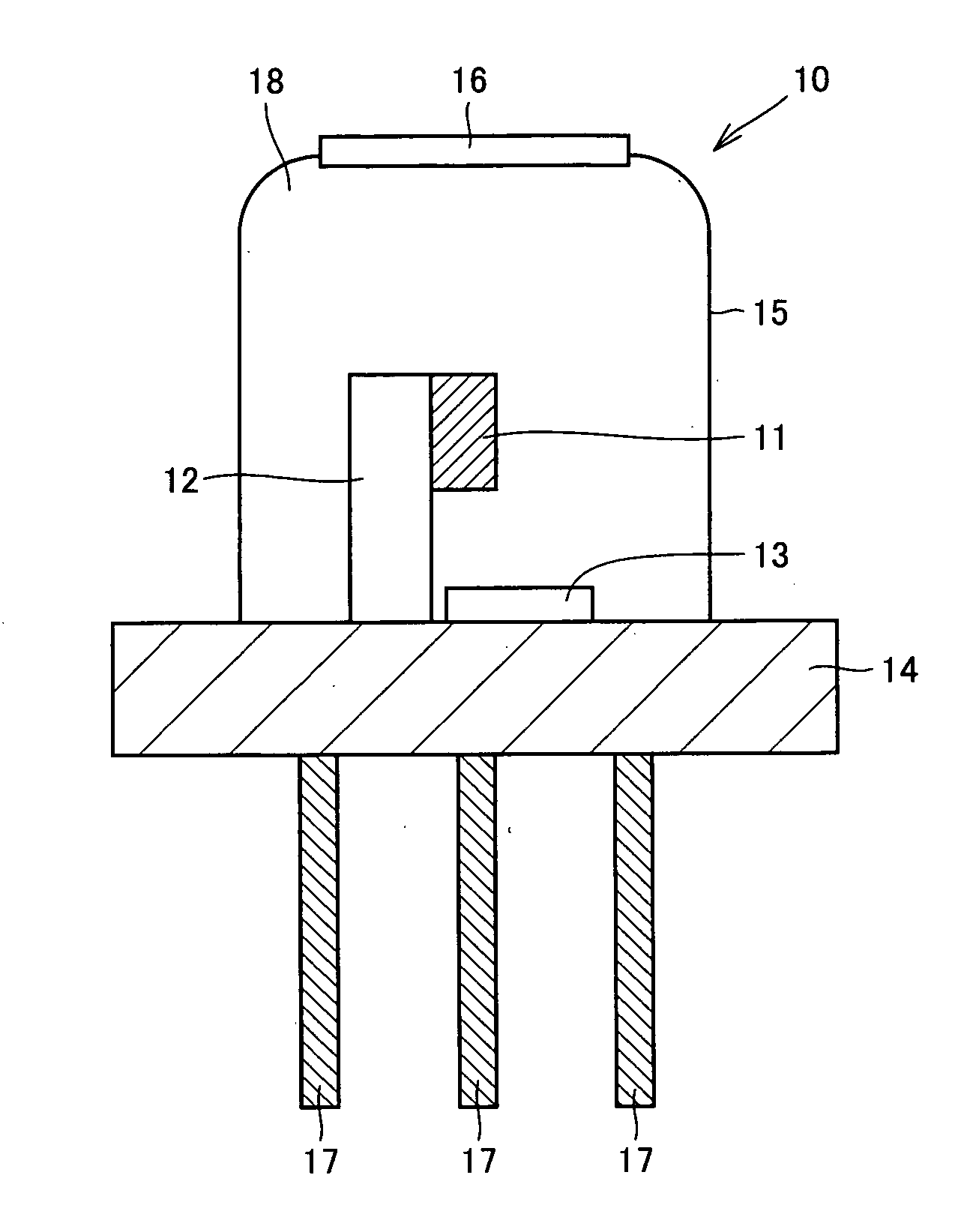
[0078] The nitride semiconductor laser device of the present invention in Example 3 is described in connection with FIG. 6. FIG. 6 is a schematic diagram of the nitride semiconductor laser device of the present invention without the light detecting element. Referring to FIG. 6, nitride semiconductor laser device 10 of the present invention includes a nitride semiconductor laser element 11 emitting a laser beam, a heat sink 12 having an end on which the nitride semiconductor laser element is provided, a stem 14 joined to the bottom surface of heat sink 12, and a cap 15 for enclosing therein nitride semiconductor laser element 11 and heat sink 12. The internal space of cap 15 is filled with an enclosed atmosphere 18. Further, ele...


PUM


Abstract

A nitride semiconductor laser device includes a nitride semiconductor laser element having a resonator end surface and capable of emitting light with a wavelength of at most 420 nm, a heat sink joined to the nitride semiconductor laser element, a stem with the heat sink mounted thereon, and a light detecting element mounted on the stem for detecting a laser beam from the nitride semiconductor laser element. The nitride semiconductor laser element, the heat sink and the light detecting element are enclosed within a cap that is joined to the stem, and an atmosphere within the cap has a dew point of at most −30° C. and an oxygen concentration of at most 100 ppm.

Description

[0001] This nonprovisional application is based on Japanese Patent Application No. 2004-156306 and 2005-086730 filed with the Japan Patent Office on May 26, 2004 and Mar. 24, 2005, respectively, the entire contents of which are hereby incorporated by reference. BACKGROUND OF THE INVENTION [0002] 1. Field of the Invention [0003] The present invention relates to a nitride semiconductor laser device, and particularly to a nitride semiconductor laser device having a characteristic in an atmosphere within a cap in which a nitride semiconductor laser element is enclosed. [0004] 2. Description of the Background Art [0005] A conventional semiconductor laser device that can be installed in a vacuum environment or high-pressure environment is disclosed in Japanese Patent Laying-Open No. 10-313147. Details of the disclosed semiconductor laser device are as follows. Referring to FIG. 4, a semiconductor laser source disclosed in Japanese Patent Laying-Open No. 10-313147 includes such components ...

Claims


Application Information

Patent Timeline
Patent Type & Authority Applications(United States)
IPC IPC(8): H01L21/00H01S5/02H01S5/022H01S5/024H01S5/0683H01S5/323
CPCH01S5/02212H01S5/0222H01S5/32341H01S5/0683H01S5/02476
Inventor TSUDA, YUHZOHHANAOKA, DAISUKEISHIDA, MASAYA
Owner SHARP FUKUYAMA LASER CO LTD
Why Eureka
Try Eureka