
Methods and systems for structured ASIC electronic design automation

a structured asic and electronic design technology, applied in the field of electronic design automation, can solve the problems of complex structure asic design constraints, eda processes that are extremely complex and consume substantial computational resources,

Inactive Publication Date: 2005-12-01
TERA SYST
View PDF9 Cites 33 Cited by
  • Summary
  • Abstract
  • Description
  • Claims
  • Application Information

AI Technical Summary

Benefits of technology

[0012] The flattened objects are clustered to accommodate design constraints associated with the structured ASIC. The design constraints can include external constraints and / or implicit constraints. For example, and without limitation, the clustering can include clustering objects having similar clock usage requirements, limiting the numbers of similar objects in a cluster, clustering objects based on area or region constraints, and / or clustering objects based on one or more cloud constraints. The clustering optionally seeks to minimize the number of interconnections between the clusters.

Problems solved by technology

EDA processes tend to be extremely complex and consume substantial computational resources.
Because of the pre-fabricated integrated circuitry, however, structured ASICs are burdened with complex design constraints, such as clock usage constraints (e.g., a finite number of clocks available in a particular area) and component constraints (e.g., finite number of flip-flops or other devices within a particular area).

Method used


Image

  • Methods and systems for structured ASIC electronic design automation
  • Methods and systems for structured ASIC electronic design automation
  • Methods and systems for structured ASIC electronic design automation

Examples


Embodiment Construction

[0024] While specific configurations and arrangements are discussed, it should be understood that this is done for illustrative purposes only. A person skilled in the pertinent art will recognize that other configurations and arrangements can be used without departing from the spirit and scope of the present invention. It will be apparent to a person skilled in the pertinent art that this invention can also be employed in a variety of other applications.

[0025] I. Integrated Circuit Design Overview

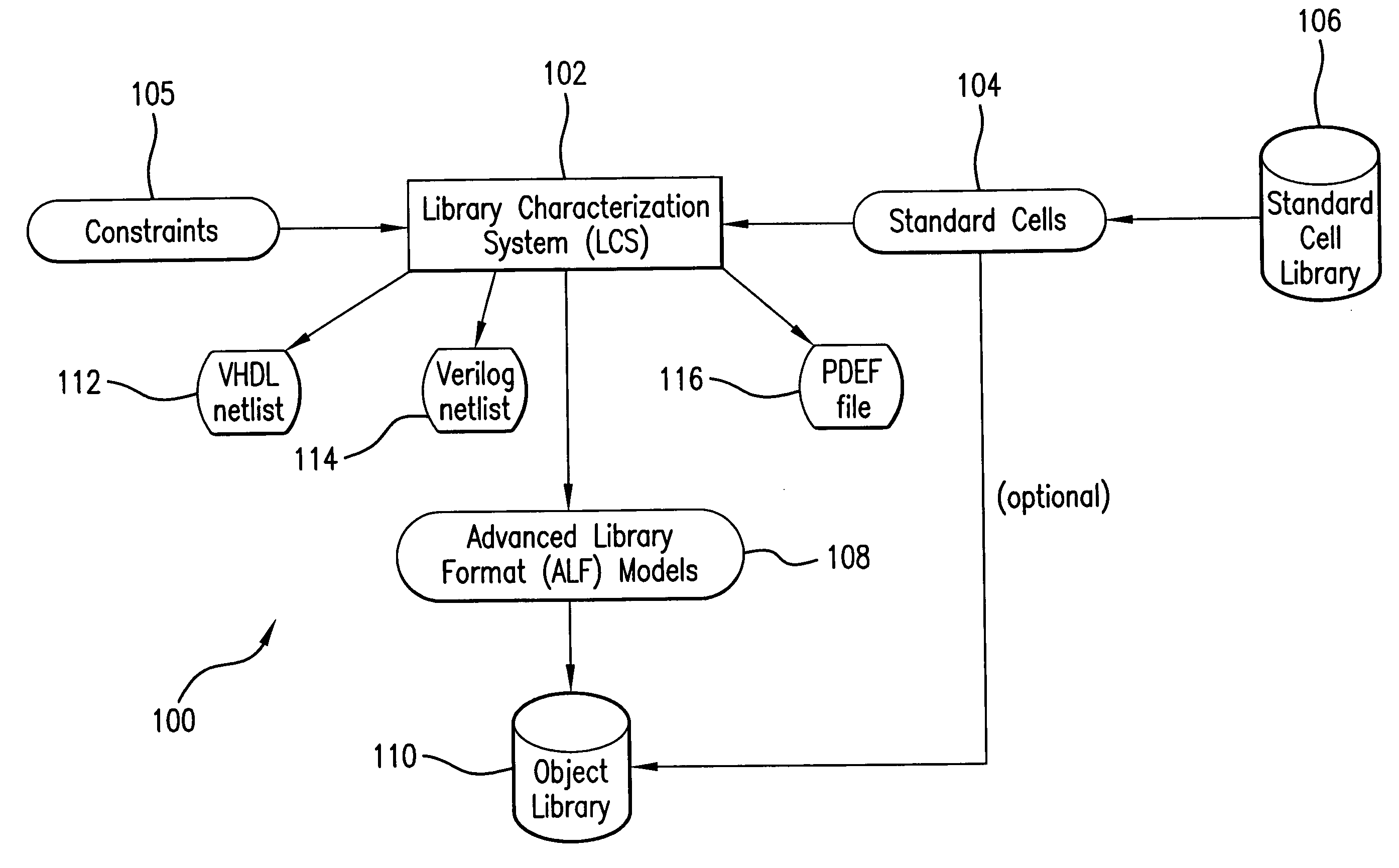
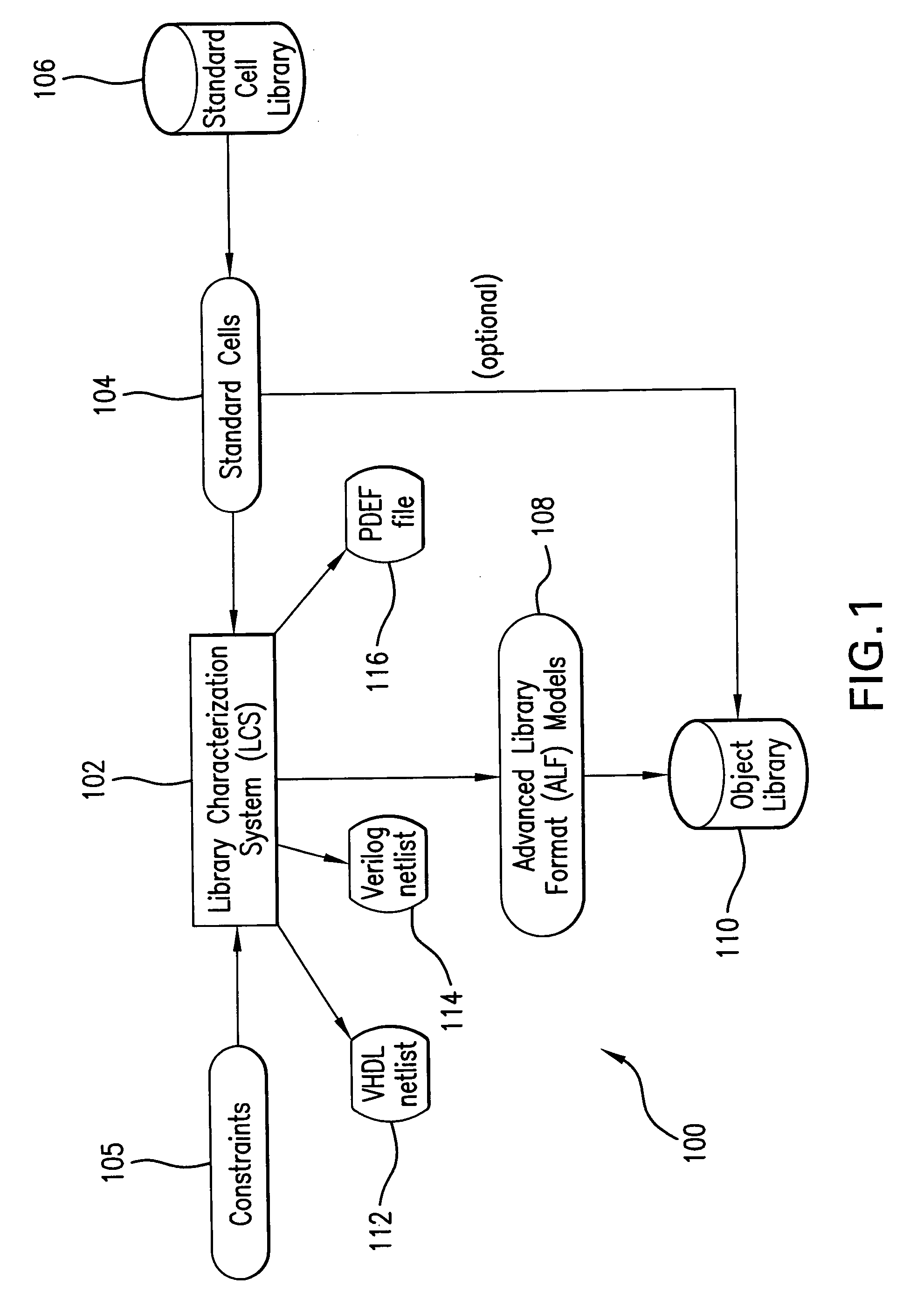
[0026] Integrated circuits are designed using computer-based hardware description languages (“HDLs”). Several types of HDL exist, including but not limited to verilog, VHDL, systemC, SystemVerilog, and resistor transistor logic (“RTL”). Although the present application will describe the invention with reference to RTL code, a person of ordinary skill in the art will recognize that any type of logic source code may be used.

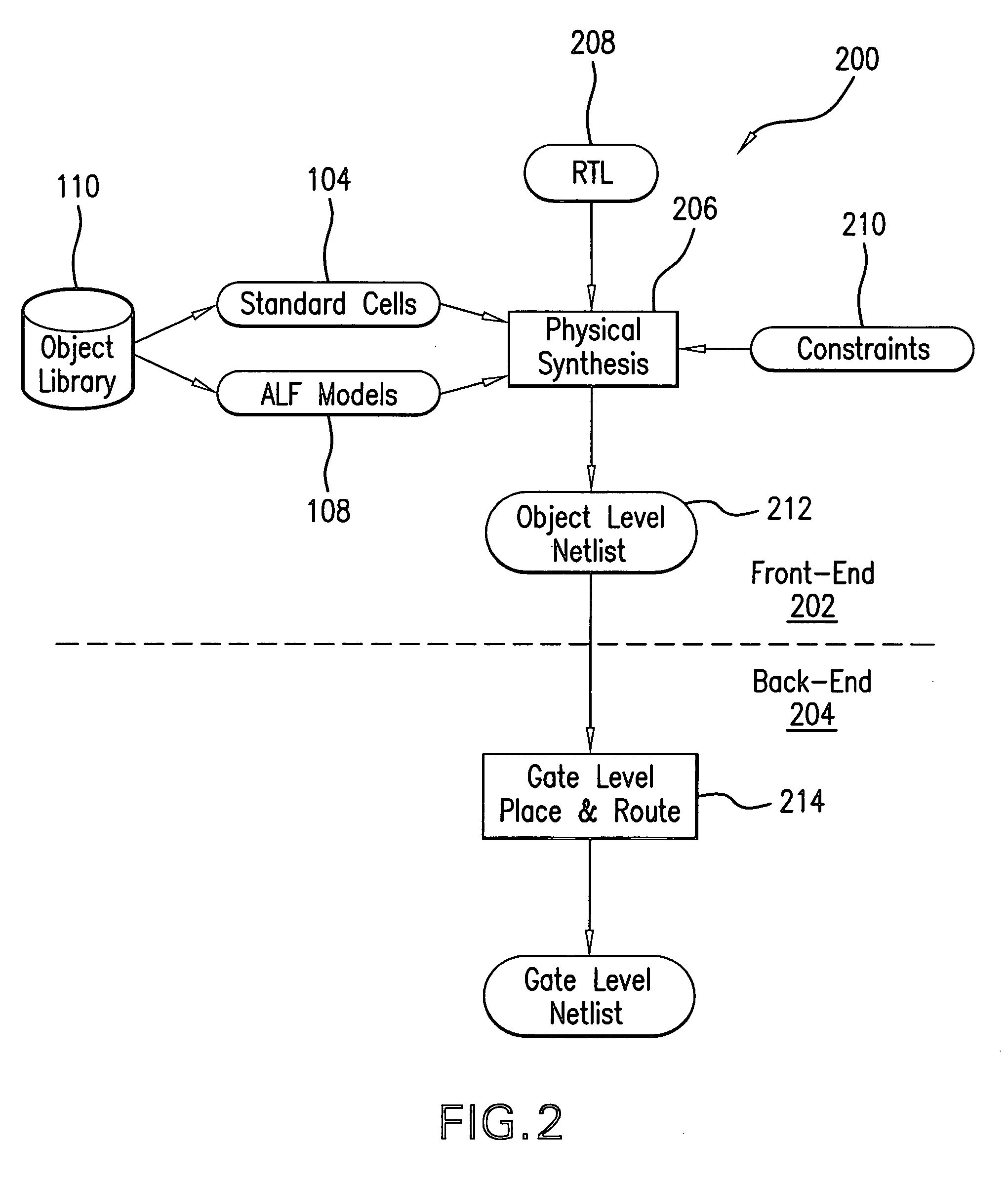
[0027] EDA tools are typically classified as front-end or back-end...


PUM


Abstract

Electronic design automation (“EDA) methods and systems for structured ASICs include accessing or receiving objects representative of source code for a structured ASIC. The objects are flattened to remove hierarchies associated with the source code, such as functional RTL hierarchies. The flattened objects are clustered to accommodate design constraints associated with the structured ASIC. The clustered objects are floorplanned within a design area of the structured ASIC. The objects are then placed within the portions of the design areas assigned to the corresponding clusters. The objects optionally include logic objects and one or more memory objects and / or proprietary objects, wherein the one or more memory objects and / or proprietary objects are placed concurrently with the logic objects.

Description

CROSS-REFERENCE TO RELATED APPLICATIONS [0001] The present invention claims the benefit of U.S. Provisional Application No. 60 / 575,422, filed Jun. 1, 2004, which is hereby incorporated by reference in its entirety.BACKGROUND OF THE INVENTION [0002] 1. Field of the Invention [0003] The invention relates to electronic design automation and, more particularly, to structured ASIC design. [0004] 2. Related Art [0005] Integrated circuits are designed using computer-based hardware description languages (“HDLs”), which are analogous to computer program source code. Electronic design automation (“EDA”) tools are used to reduce the HDL code to actual integrated circuit designs. The integrated circuit designs can then be fabricated into integrated circuits. Reduction of HDL code to a circuit design is analogous to the reduction (i.e., compiling) of computer program source code to machine language code. EDA processes can “reduce” hundreds or thousands of lines of HDL code to millions of transis...

Claims


Application Information

Patent Timeline
IPC IPC(8): G06F9/45G06F17/50
CPCG06F17/5045G06F2217/64G06F17/5068G06F17/505G06F2115/06G06F30/39G06F30/327G06F30/30
Inventor WANG, TENG-ISHANG, ZHONG-QING
Owner TERA SYST
Learn More