
Tb, b-based yellow phosphor, its preparation method, and white semiconductor light emitting device incorporating the same

a yellow phosphor and terbium borate technology, applied in the field of semiconductor light emitting devices, can solve the problems of difficult control of current strength, reducing the overall light emitting efficiency, and difficult to construct three rgb leds on a single chip, so as to improve the emitting luminance and color rendering, reduce the degree of deterioration in emission intensity, and improve the effect of emission efficiency and color shi

Inactive Publication Date: 2005-12-08
LUXPIA
View PDF3 Cites 19 Cited by
  • Summary
  • Abstract
  • Description
  • Claims
  • Application Information

AI Technical Summary

Benefits of technology

[0012] Thus, an object of the present invention is to solve the problems described above and provide a phosphor that can improve the emitting luminance and color rendering of a white light emitting device, a preparation method thereof, and a white semiconductor light emitting device which experiences only extremely low degrees of deterioration in emission intensity, emission efficiency and color shift over a long period of service and implements wide range of colors.

Problems solved by technology

According to this method, it is difficult to constructing three RGB LEDs on a single chip and it is difficult to control a current strength because each LED is made from different material and by different method, and driving voltage of each LED is different.
However, the above two methods have the following problems: a satisfactory material to obtain green light has not been developed as yet; and light emitted from the blue LED may be absorbed by the red LED to lower the overall light emitting efficiency.

Method used


Image

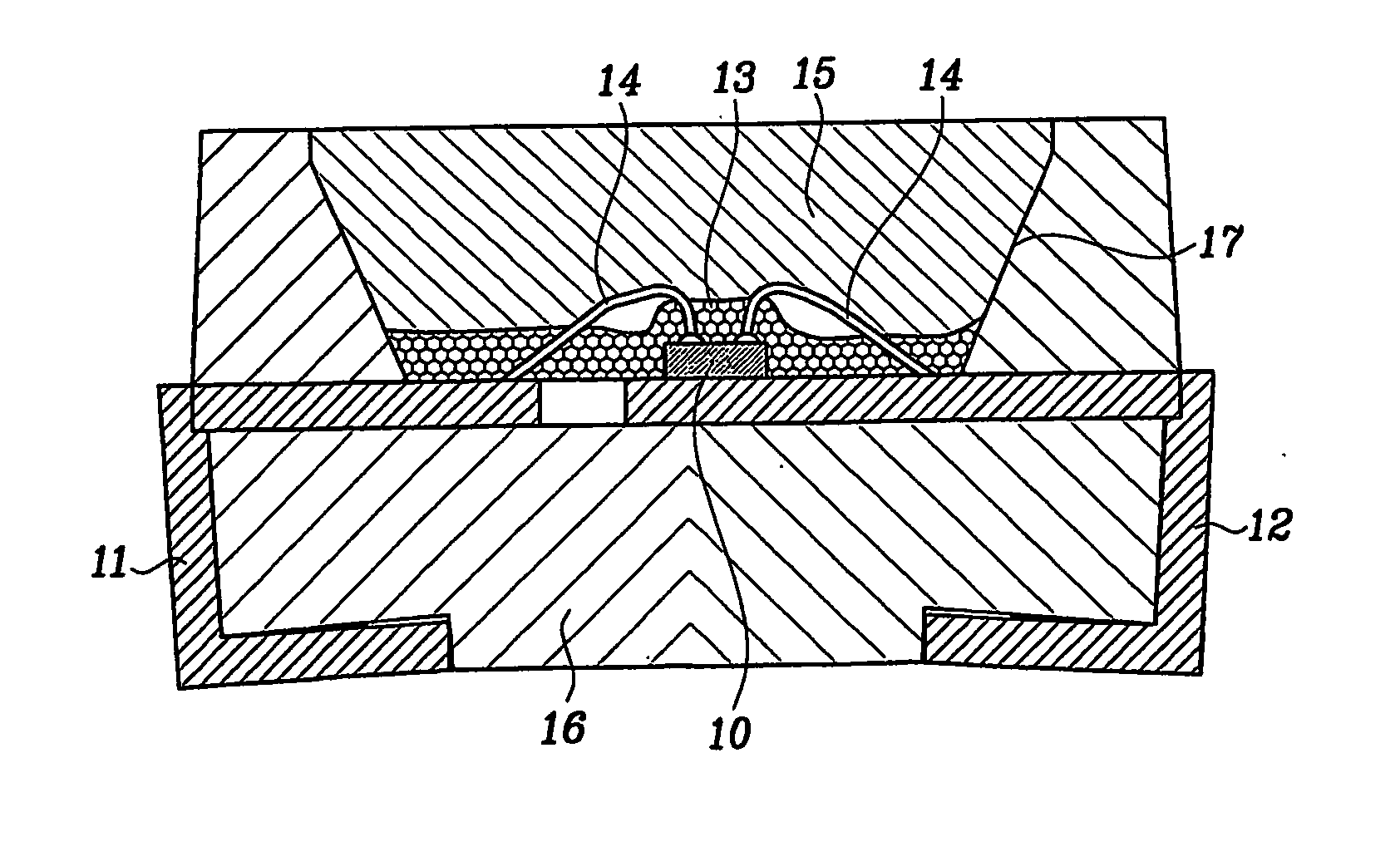
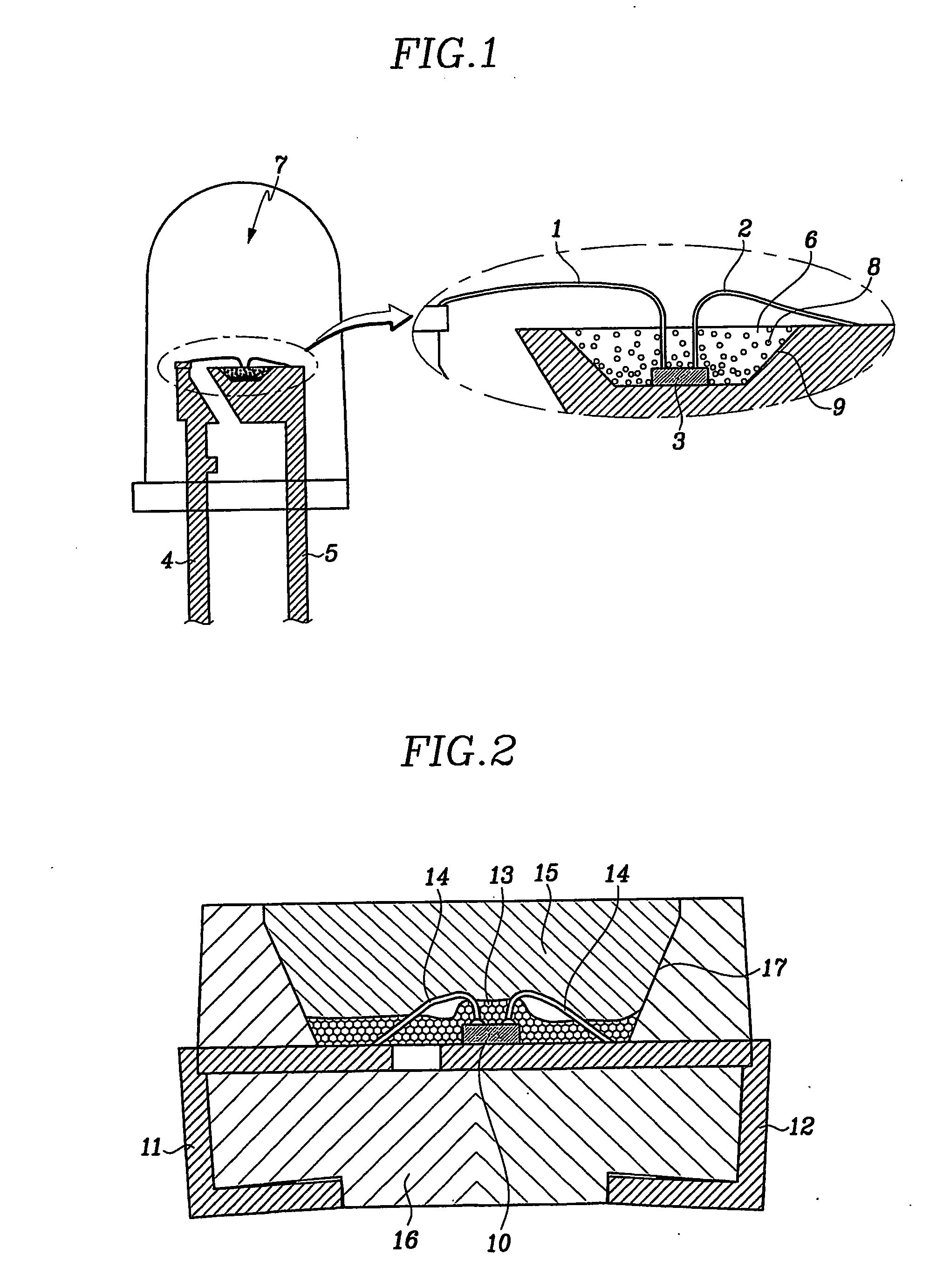
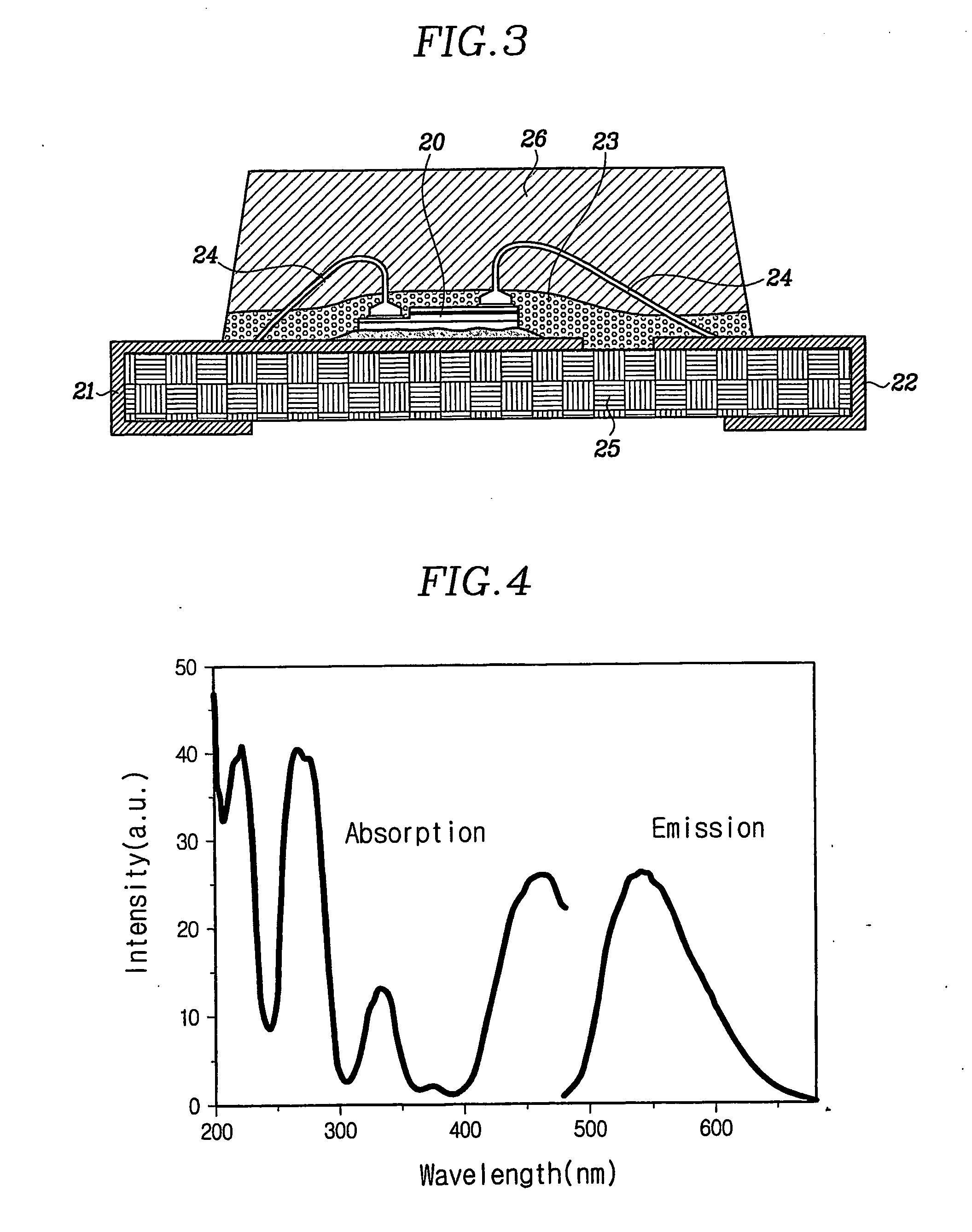
  • Tb, b-based yellow phosphor, its preparation method, and white semiconductor light emitting device incorporating the same
  • Tb, b-based yellow phosphor, its preparation method, and white semiconductor light emitting device incorporating the same
  • Tb, b-based yellow phosphor, its preparation method, and white semiconductor light emitting device incorporating the same

Examples


Embodiment Construction

[0027] Hereinafter, the present invention is described in more detail.

[0028] The yellow phosphor provided by the present invention comprises cerium-activated terbium, boron and an amphoteric typical element, and as the amphoteric typical element, Al, In, Ga or their mixture is used.

[0029] Preferably, the yellow phosphor of the present invention is a terbium borate-based phosphor represented by the following general formula:

(Tb1-x-y-zRexAy)3DaBbO12:Cez

[0030] In the formula, RE is at least one rare earth element selected from the group consisting of Y, Lu, Sc, La, Gd, Sm, Pr, Nd, Eu, Dy, Ho, Er, Tm and Yb; A is at least one typical metal element selected from the group consisting of Li, Na, K, Rb, Cs and Fr, D is at least one typical amphoteric element selected from the group consisting of Al, In and Ga; 0≦x<0.5; 0≦y<0.5; 0<z<0.5; 0<a<5; and 0<b<5.

[0031] Preferably, x, y, and z are selected to satisfy: 0


PUM


Abstract

The present invention relates to a terbium borate-based yellow phosphor, a preparation method thereof, and a white semiconductor light emitting device incorporating the same. The terbium borate-based yellow phosphor of the present invention is represented by the general formula (Tb1-x-y-zREXAy)3DaBbO12:Cez (where, RE is at least one rare earth element selected from the group consisting of Y, Lu, Sc, La, Gd, Sm, Pr, Nd, Eu, Dy, Ho, Er, Tm and Yb; A is a typical metal element selected from the group consisting of Li, Na, K, Rb, Cs and Fr; D is a typical amphoteric element selected from the group consisting of Al, In and Ga; 0≦x<0.5; 0≦y<0.5; 0<z<0.5; 0<a<5; and 0<b<5). The white semiconductor light emitting device of the present invention comprises a semiconductor light emitting diode and the yellow phosphor, which absorbs a portion of light emitted by the semiconductor light emitting diode and emits light of wavelength different from that of the absorbed light. It offers white light from the combination of the light emitted by the semiconductor light emitting diode and the light emitted by the yellow phosphor. The white semiconductor light emitting device of the present invention offers a greatly improved color rendering and experiences less deterioration in light emission efficiency over a long period of service.

Description

BACKGROUND OF THE INVENTION [0001] (a) Field of the Invention [0002] The present invention relates to a semiconductor light emitting device. More particularly, it relates to a terbium borate-based yellow phosphor, a preparation method thereof, and a semiconductor light emitting device incorporating the yellow phosphor which absorbs a portion of light emitted by a light emitting diode, and emits light of wavelength different from that of the absorbed light, thereby implementing such white light as purely white light and bluish white light by incorporating the yellow phosphor. [0003] (b) Description of the Related Art [0004] A semiconductor light emitting diode (LED) is a PN-junctioned compound semiconductor. It is a kind of optoelectronic device that emits light energy corresponding to the band gap of a semiconductor generated by a combination of an electron and a hole when a voltage is applied. [0005] As full colorization of LED was realized with the development of high luminance bl...

Claims


Application Information

Patent Timeline
IPC IPC(8): C09K11/77C09K11/78H01L29/24H01L33/50
CPCC09K11/778H01L33/502Y02B20/181H01L2224/48091H01L2224/48247H01L2224/8592H01L2224/49107H01L2224/73265H01L2924/00014Y02B20/00
Inventor LEE, DONG-YEOULKIM, YONG-TAEKIM, JIN-HWANKIM, EUN-JOUNG
Owner LUXPIA
Learn More