Transistors amd methods for making the same

Active Publication Date: 2005-12-08
ALCATEL-LUCENT USA INC +1
View PDF5 Cites 16 Cited by
  • Summary
  • Abstract
  • Description
  • Claims
  • Application Information

AI Technical Summary

Benefits of technology

[0012] The present invention provides heterobipolar transistors comprising multilayer structures each including a collector, a base and an emitter, and further comprising a base electrode located at a controlled charge carrier access path distance from the emitter. This controlled access path distance facilitates a reduced base

Problems solved by technology

As the maximum available processing speeds of such devices continually grow, the demand for transistors facilitating still greater processing speeds likewise grows unabated.
Such si

Method used


Image

  • Transistors amd methods for making the same
  • Transistors amd methods for making the same
  • Transistors amd methods for making the same

Examples


Embodiment Construction

[0019] The present invention will now be described more fully with reference to the accompanying drawings, in which several presently preferred embodiments of the invention are shown. This invention may, however, be embodied in various forms and should not be construed as being limited to the embodiments set forth herein.

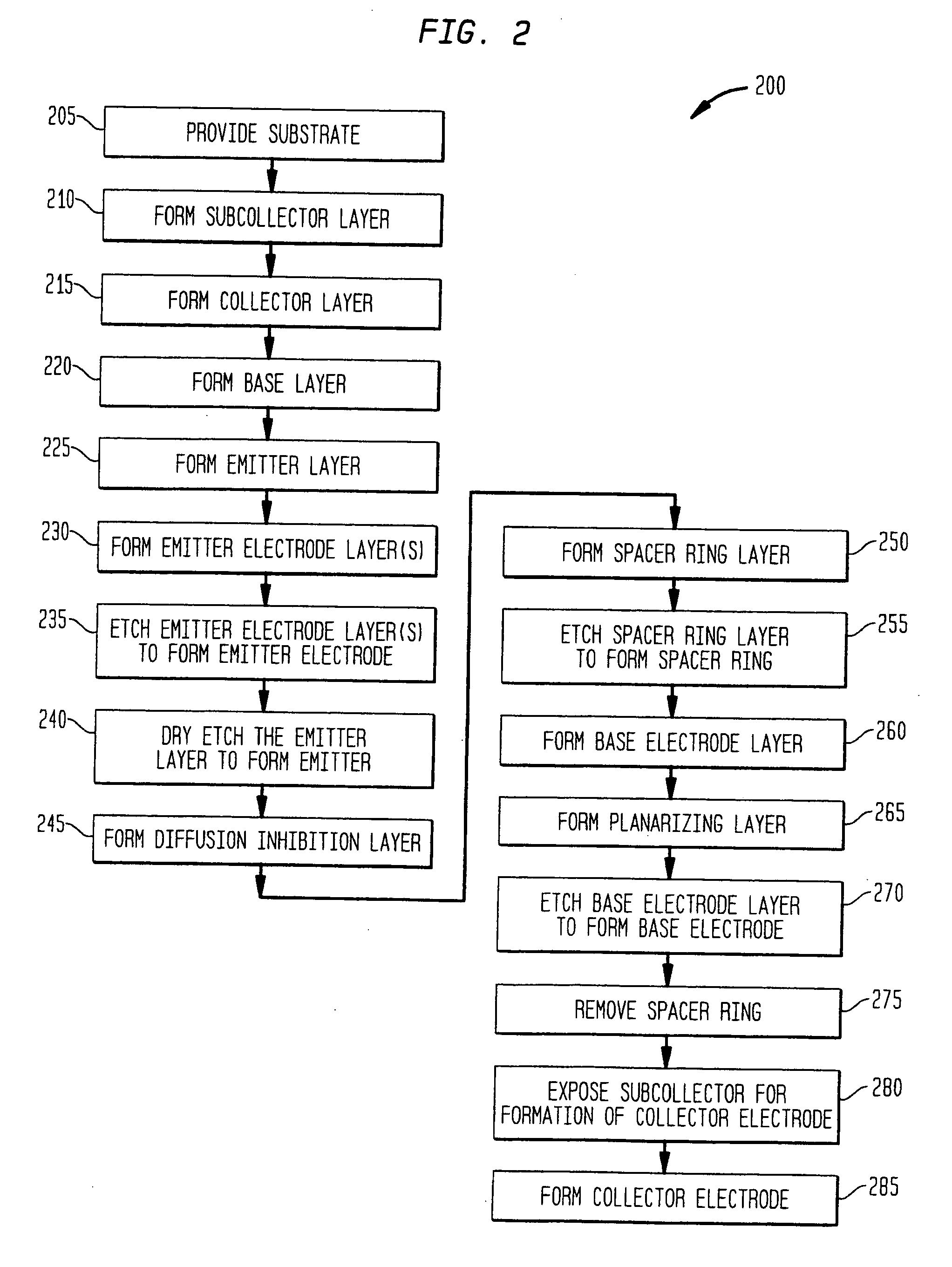
[0020] The present invention provides HBTs comprising base electrodes separated by defined vertical and horizontal distances from an adjacent emitter or collector. A space that directly spans such distances may be occupied by ambient air or by another dielectric material. The present invention further provides processes for making such HBTs, comprising the formation of a spacer ring that facilitates accurate self aligned preparation of the base electrodes.

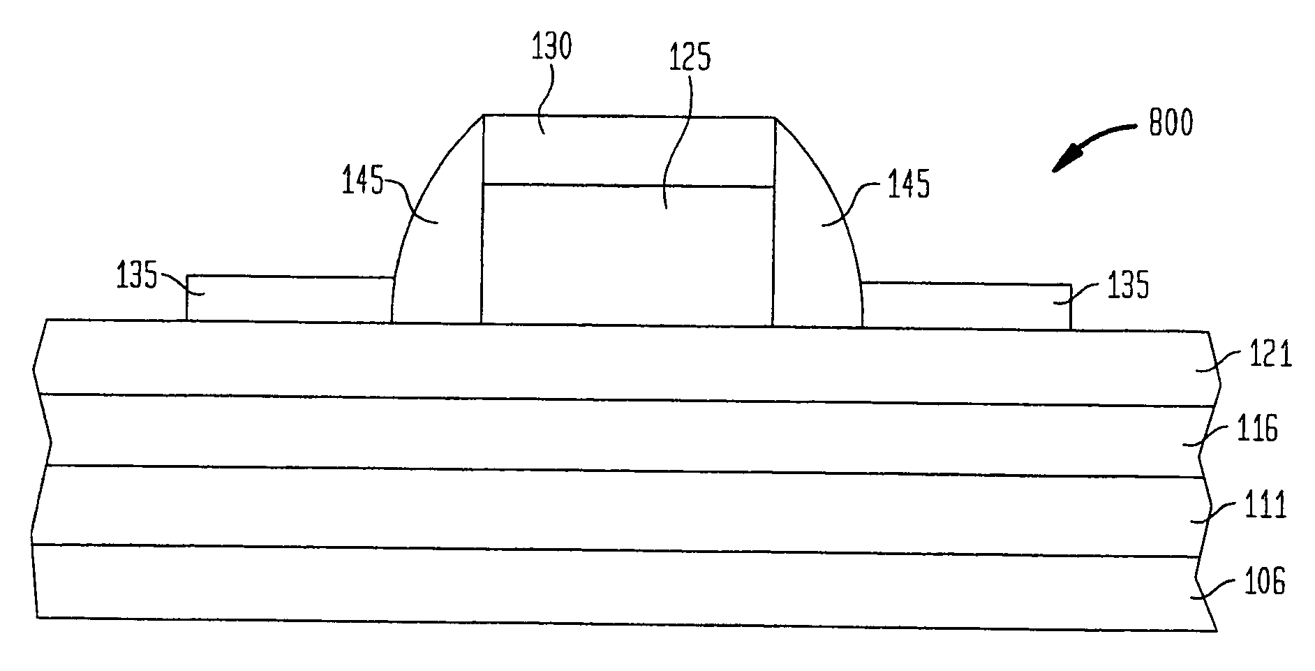
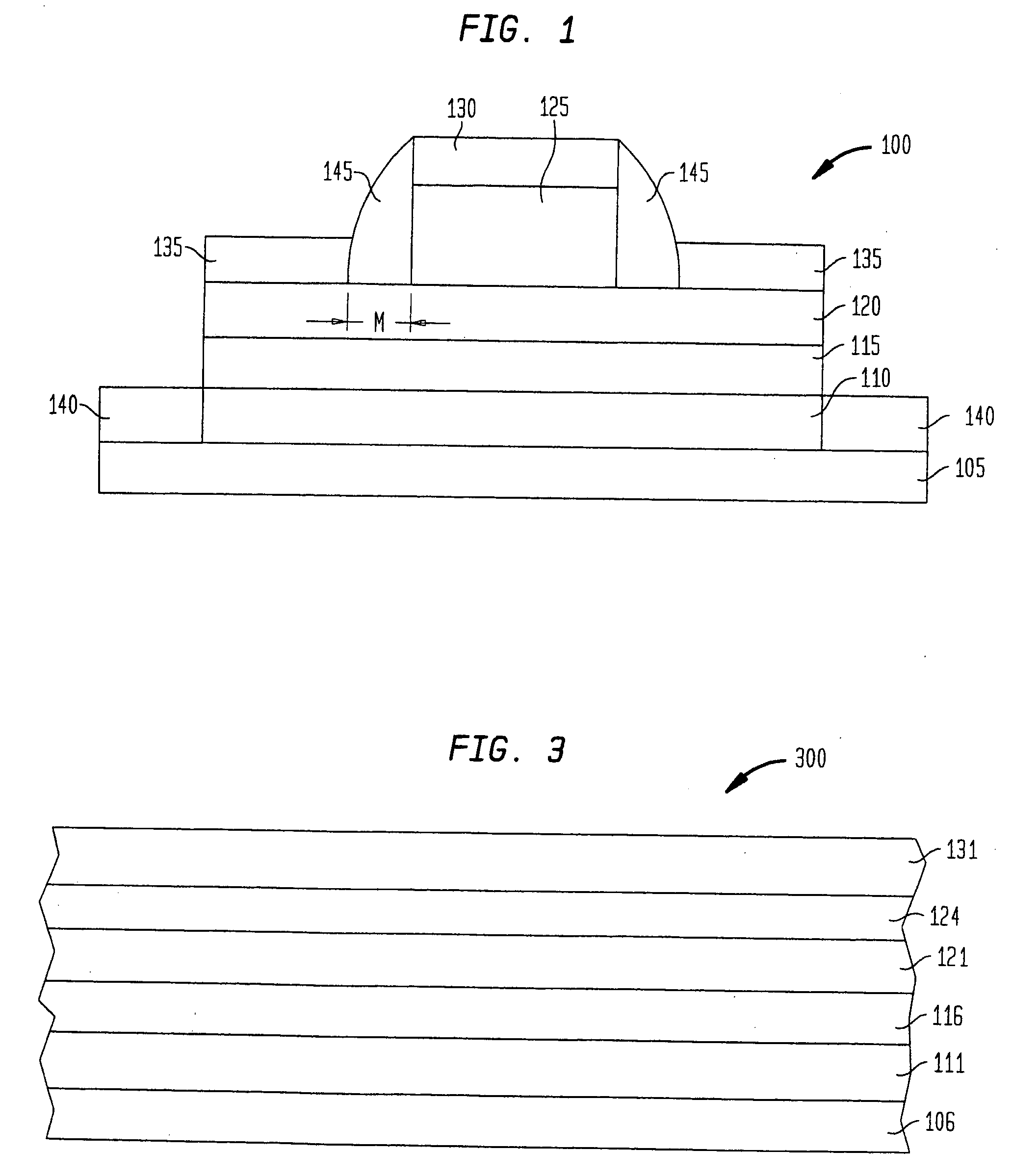
[0021]FIG. 1 shows a cross section of an HBT 100 in accordance with the present invention. The HBT 100 comprises a multilayer structure comprising a substrate 105, a subcollector 110, a collector 115, a base 120,...


PUM


Abstract

Apparatus comprising: a first compound semiconductor composition layer doped to have a first charge carrier polarity; a second compound semiconductor composition layer doped to have a second charge carrier polarity and located on the first layer; a third compound semiconductor composition layer doped to have the first charge carrier polarity and located on the second layer; a base electrode on the second layer; and a spacer ring interposed between and defining a charge carrier access path distance between the base electrode and the third layer, the path distance being within a range of between about 200 Å and about 1000 Å. Techniques for making apparatus. Apparatus is useful as a heterobipolar transistor, particularly for high frequency applications.

Description

[0001] The U.S. Government has a paid-up license in this invention and the right in limited circumstances to require the patent owner to license others on reasonable terms as provided for by the terms of U.S. Defense Advanced Research Projects Agency (“DARPA”) TFAST contract No. MDA972-03-C-0027.FIELD OF THE INVENTION [0002] This invention relates to the fields of transistors, methods of making transistors, and integrated circuits comprising transistors. BACKGROUND OF THE INVENTION [0003] Transistors in vast quantities linked into massive integrated circuits form the backbones of microprocessors and other high speed active electronic devices. As the maximum available processing speeds of such devices continually grow, the demand for transistors facilitating still greater processing speeds likewise grows unabated. A fundamental strategy for delivering such ever increasing speed involves progressively scaling down the transistor dimensions. [0004] Heterobipolar transistors (“HBTs”) ar...

Claims


Application Information

Patent Timeline
IPC IPC(8): H01L21/331H01L21/8222H01L29/732H01L29/737H01L31/0328H01L31/0336H01L31/072H01L31/109
CPCH01L29/66242H01L29/7371H01L29/66318
Inventor CHEN, YOUNG-KAIHOUTSMA, VINCENT ETIENNEWEIMANN, NILS GUENTER
Owner ALCATEL-LUCENT USA INC
Why Eureka
Try Eureka