Semiconductor device and manufacturing method thereof

a technology of semiconductors and semiconductors, applied in the direction of semiconductor devices, electrical devices, transistors, etc., can solve the problem of not paying attention to sti stress, and achieve the effect of suppressing the generation of crystal defects in the substra

Inactive Publication Date: 2005-12-08
RENESAS ELECTRONICS CORP
View PDF2 Cites 8 Cited by
  • Summary
  • Abstract
  • Description
  • Claims
  • Application Information

AI Technical Summary

Benefits of technology

[0005] An object of the present invention is to provide a semiconductor device and manufacturing method thereof capable of overcoming the above-described inconvenience.
[0006] With a view to overcoming the above-described problem, the semiconductor device of the present invention has a structure in which an external stress from an element isolation region is reduced, which makes it possible to suppress crystal defects which occur in a semiconductor substrate in the vicinity of a region into which impurities for source and drain have been implanted.
[0009] Even if diffusion layers such as source and drain have been formed by ion implantation, generation of crystal defects in the substrate can be suppressed by adopting the above-described constitution. Stress concentration due to growth of an oxide film on the sidewalls of the trench by oxidation of the trench can therefore be relaxed at least by making the element isolation insulating film more porous than the thermal oxide film (surface film of the trench).
[0010] In another aspect, it is also possible to form the element isolation insulating film buried in the element isolation trench and the gate insulating film as a film having silicon oxide as their main constituent element, and make the element isolation insulating film more porous than the gate insulating film.
[0030] In this semiconductor device, the surface of a buried oxide film in the element isolation region is made lower than the substrate surface in the element formation region, which makes it possible to effectively suppress the generation of crystal defects.
[0046] According to the present invention, a semiconductor device and a manufacturing method thereof capable of contributing to elimination of the above-described inconvenience can be provided.

Problems solved by technology

In the above-described patent document, however, no consideration is paid for the STI stress.

Method used


Image

  • Semiconductor device and manufacturing method thereof
  • Semiconductor device and manufacturing method thereof
  • Semiconductor device and manufacturing method thereof

Examples


first embodiment

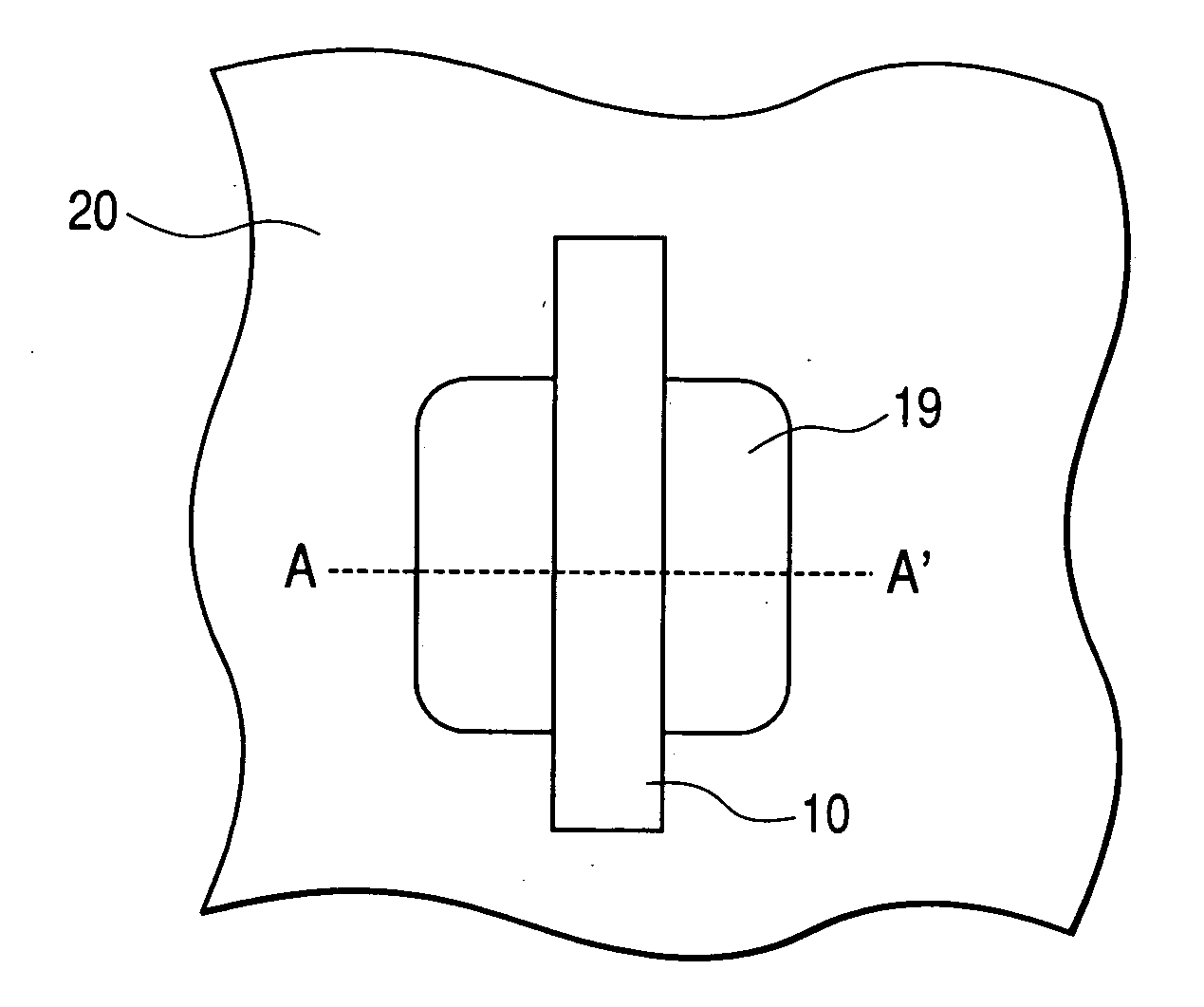
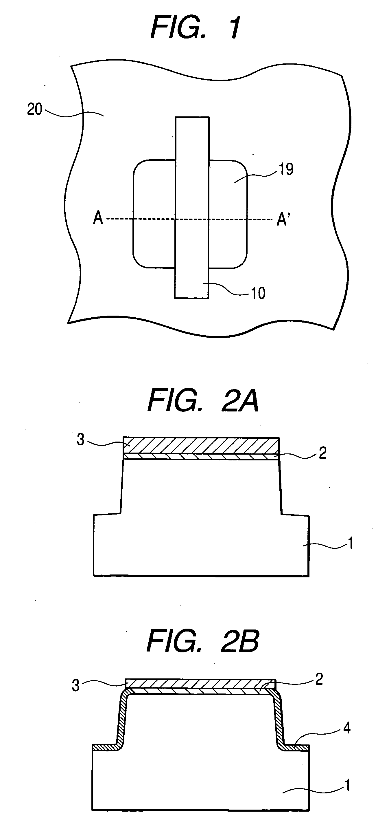
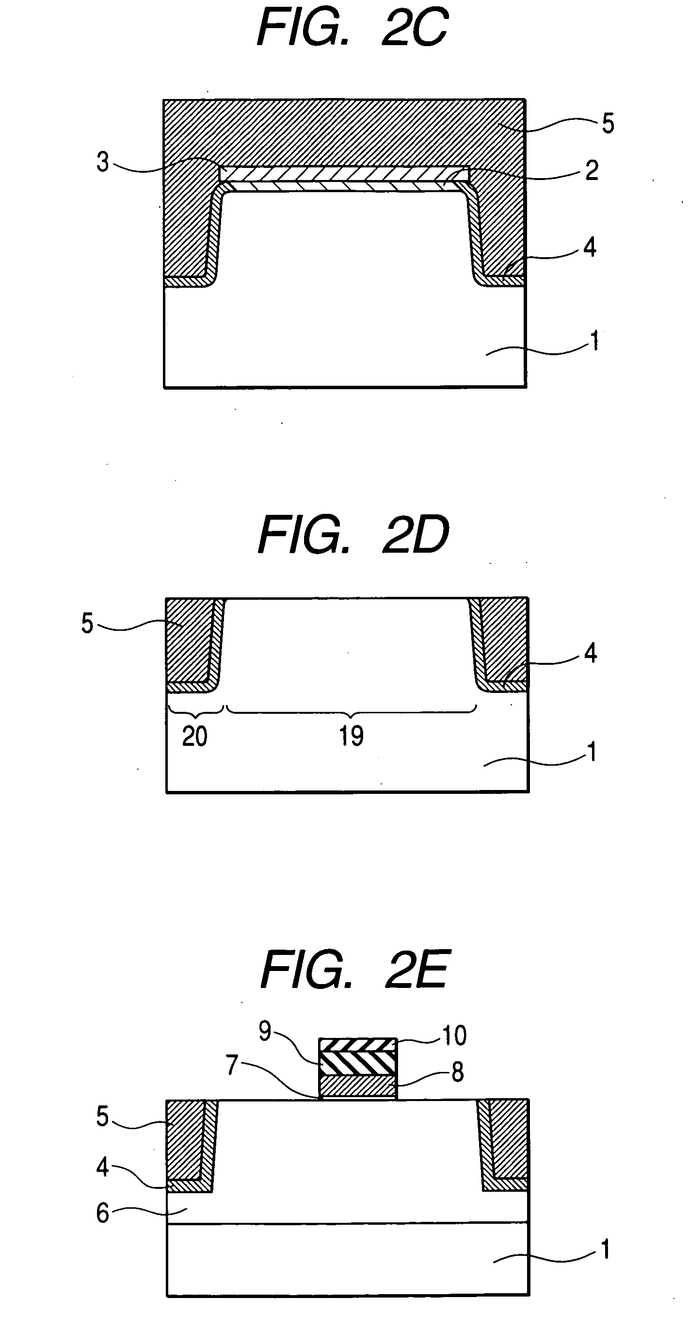
[0069] Manufacturing steps of a semiconductor device according to the present invention will next be described referring to FIGS. 1 to 2J.

[0070]FIG. 1 is a plan layout view and FIG. 2 is across-sectional view of the structure taken along a line A-A′ of FIG. 1.

[0071] (1) A pad oxide film 2 having a thickness of from 5 to 15 nm and a silicon nitride film 3 having a thickness of about 150 nm are deposited over a silicon substrate 1. Desired portions of the silicon nitride film 3, pad oxide film 2 and silicon substrate 1 are partly removed by etching, whereby shallow trenches each having a predetermined angle between the silicon substrate 1 and surface sidewall of the silicon substrate 1 are formed (FIG. 2A).

[0072] (2) The surface of the silicon substrate 1 is thermally oxidized in an oxidizing atmosphere at a temperature range of from 900 to 1150° C. to form an element isolation thermal oxide film 4 having a thickness of several nm to several tens nm in the trenches (FIG. 2B). The tr...

third embodiment

[0107]FIGS. 7 and 8 illustrate the present invention.

[0108] A semiconductor device according to the third embodiment is principally similar to that of the second embodiment. The device of the third embodiment has, in the element formation region, an impurity region obtained by implanting an impurity into the semiconductor substrate relative to the gate electrode and the interface of the second element isolation insulating film on the side of the interlayer insulating film 15 and on the side of the first element isolation film are formed in a region deeper than the depth which is below the surface of the substrate in the impurity region and at which an impurity concentration becomes highest. The first element isolation insulating film has a surface, on the side of the interlayer insulating film, formed in a region deeper the above-described region.

[0109] More specifically, the surface (FIG. 7) of the buried insulating film 5 on the side of the interlayer insulating film 15 or, when ...


PUM


Abstract

To suppress occurrence of dislocation in a substrate of a semiconductor device at an end portion of a gate electrode. Provided is a semiconductor device having a plurality of element formation regions formed over the main surface of a semiconductor substrate, an element isolation trench located between the element formation regions and having an element isolation insulating film embedded therein, and a gate insulating film, a gate electrode and a plurality of interconnect layers formed thereabove, each formed in the element formation region, wherein the element isolation trench has a thermal oxide film formed between the semiconductor substrate and the element isolation insulating film, and the element isolation film has a great number of micro-pores formed inside thereof and is more porous than the thermal oxide film.

Description

CLAIM OF PRIORITY [0001] The present application claims priority from Japanese application serial JP 2004-154226 filed on May 25, 2004, the content of which is hereby incorporated by reference into this application. FIELD OF THE INVENTION [0002] The present invention relates to a semiconductor device and a manufacturing method thereof. BACKGROUND OF THE INVENTION [0003] An insulating film which is to be a sidewall is formed on the sidewalls of a gate electrode of an MOS transistor, and source and drain regions are formed by implanting an impurity into both sides of the gate electrode. At the end portions of these source and drain regions, however, many crystal defects appear in a silicon substrate. As a method of preventing these crystal defects, Japanese Patent Laid-Open No. H8(1996)-97210 (Patent Document 1) discloses a mode in which the influence of a stress caused by a nitride film formed on the side surface of a gate electrode is suppressed by forming an oxide film on the side ...

Claims


Application Information

Patent Timeline
Patent Type & Authority Applications(United States)
IPC IPC(8): H01L21/312H01L21/76H01L21/316H01L21/8234H01L21/8247H01L27/08H01L27/115H01L29/78H01L29/788H01L29/792
CPCH01L21/3124H01L29/7833H01L21/823481H01L21/31662H01L21/02203H01L21/02137H01L21/02134H01L21/02107H01L21/76224
Inventor ISHITSUKA, NORIOTANAKA, JUNIWASAKI, TOMIOOHTA, HIROYUKI
Owner RENESAS ELECTRONICS CORP
Why Eureka
Try Eureka