Conductor device and method of manufacturing thereof
a semiconductor and thermal resistance technology, applied in semiconductor devices, semiconductor/solid-state device details, electrical devices, etc., can solve the problems of unsolved warpage of package substrates along one direction, and the warpage of semiconductor packages can be suppressed, so as to achieve small warpage of semiconductor packages and suppress the effect of warpag
- Summary
- Abstract
- Description
- Claims
- Application Information
AI Technical Summary
Benefits of technology
Problems solved by technology
Method used
Image
Examples
first embodiment
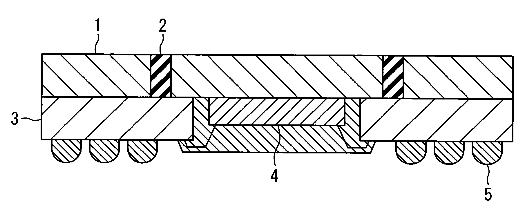
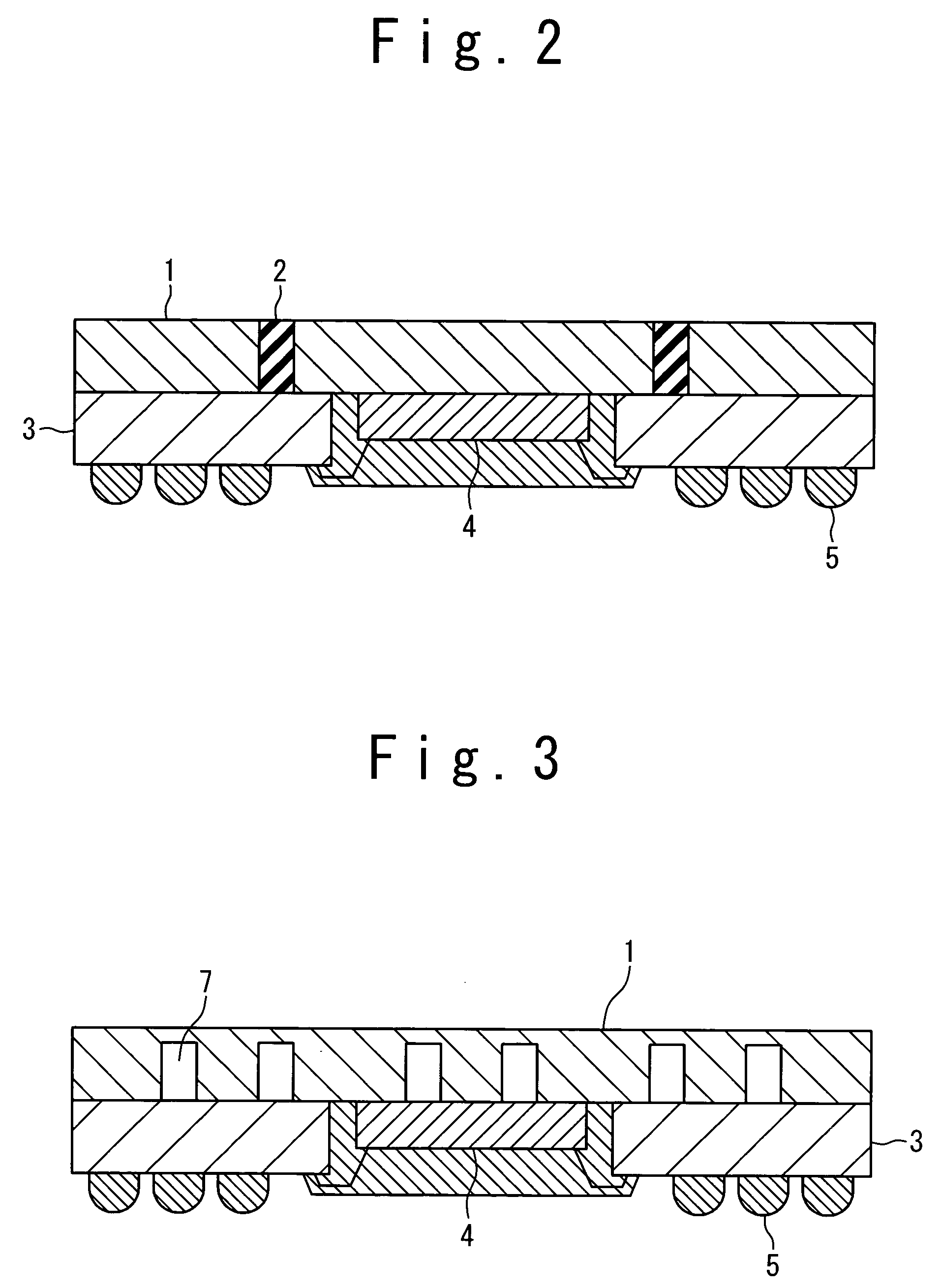
[0032] A semiconductor device according to a first embodiment of the present invention will be described below with reference to FIG. 2.
[0033]FIG. 2 is a cross-sectional view showing a structure of the semiconductor device. The semiconductor device has a package substrate 3.
[0034] A semiconductor chip 4 is accommodated in the package substrate 3, and an external terminal 5 such as a soldering ball is formed on a surface of the package substrate 3. Also, the semiconductor device has a heat spreader 1 attached to the package substrate 3 with an adhesive sheet. More specifically, a first surface of the heat spreader 1 is attached to the package substrate 3.
[0035] As shown in FIG. 2, a slit 2 is formed in the heat spreader 1. The slit 2 extends in a direction normal to a page surface. More specifically, the slit 2 has a lattice-shape when viewed from above, as will be described later. Also, the lattice-shaped slit 2 penetrates through the heat spreader 1 along the thickness direction...
second embodiment
[0037] A semiconductor device according to a second embodiment of the present invention will be described below with reference to FIG. 3. FIG. 3 is a cross-sectional view showing a structure of the semiconductor device. In the present embodiment, a lattice-shaped slit 7 instead of the above-mentioned lattice-shaped slit 2 is formed in the heat spreader 1. Here, the lattice-shaped slit 7 does not penetrate through the heat spreader 1, as shown in FIG. 3. The lattice-shaped silt 7 opens only on the first surface of the heat spreader 1. In other words, the heat spreader 1 has apertures only on the first surface which is attached to the package substrate 3. The difference in the amount of thermal expansion between the heat spreader 1 and the package substrate 3 is absorbed by the lattice-shaped slit 7. Therefore, warpage of the package substrate 3 and the semiconductor package can be suppressed and reduced. It should be noted that the lattice-shaped slit 7 may be filled with a thermal c...
third embodiment
[0038] A semiconductor device according to a third embodiment of the present invention will be described below with reference to FIGS. 4A and 4B. FIG. 4A is a cross-sectional view showing a structure of the semiconductor device. FIG. 4B is a top view of the semiconductor device as viewed from the side of the heat spreader 1. As in the first embodiment, the lattice-shaped slit 2 penetrating through the heat spreader 1 is formed. The lattice-shaped slit 2 opens on the first surface and the second surface of the heat spreader 1, as shown in FIG. 4A. The heat spreader 1 is divided into a plurality of blocks due to the lattice-shaped slit 2, as shown in FIG. 4B.
[0039] A difference between the first embodiment and the present embodiment lies in that the plurality of blocks are coupled to one another by suspension pins 6. As shown in FIG. 4B, a block of the plurality of blocks is linked by suspension pins 6 to adjacent blocks. When the plurality of blocks are linked one another, handling ...
PUM
 Abstract
Description
Claims
Application Information
 - R&D
- Intellectual Property
- Life Sciences
- Materials
- Tech Scout
- Unparalleled Data Quality
- Higher Quality Content
- 60% Fewer Hallucinations
Browse by: Latest US Patents, China's latest patents, Technical Efficacy Thesaurus, Application Domain, Technology Topic, Popular Technical Reports.
© 2025 PatSnap. All rights reserved.Legal|Privacy policy|Modern Slavery Act Transparency Statement|Sitemap|About US| Contact US: help@patsnap.com


