

Liquid crystal display with defect reparability
a liquid crystal display and defect technology, applied in non-linear optics, instruments, optics, etc., can solve the problems of significant time-consuming repair, unfavorable production, and degradation of display quality, so as to facilitate reduce the steps of laser cutting in the defect repair process, and improve the effect of quality
- Summary
- Abstract
- Description
- Claims
- Application Information
AI Technical Summary
Benefits of technology
Problems solved by technology
Method used
Image

Examples
embodiment 1
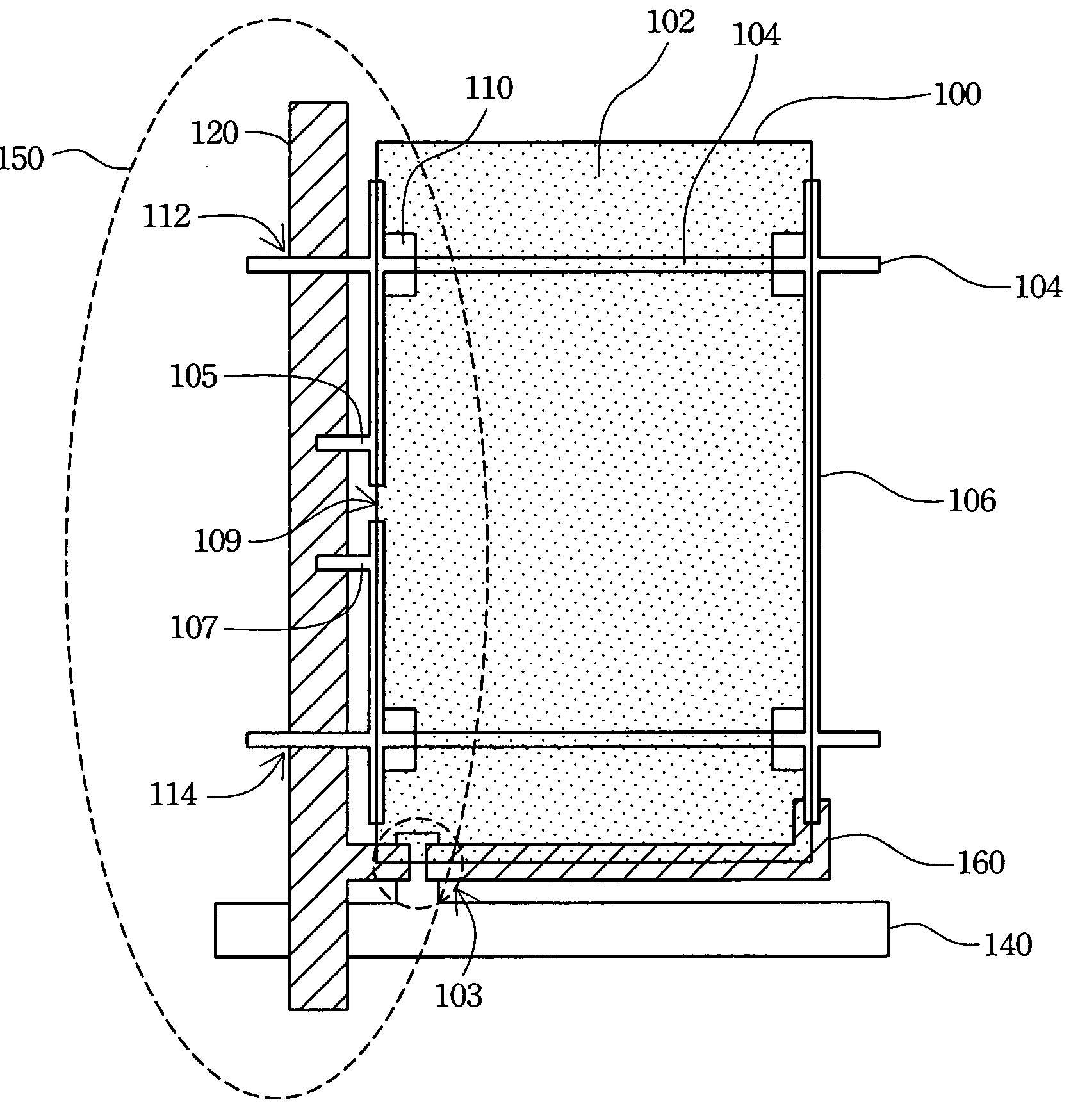
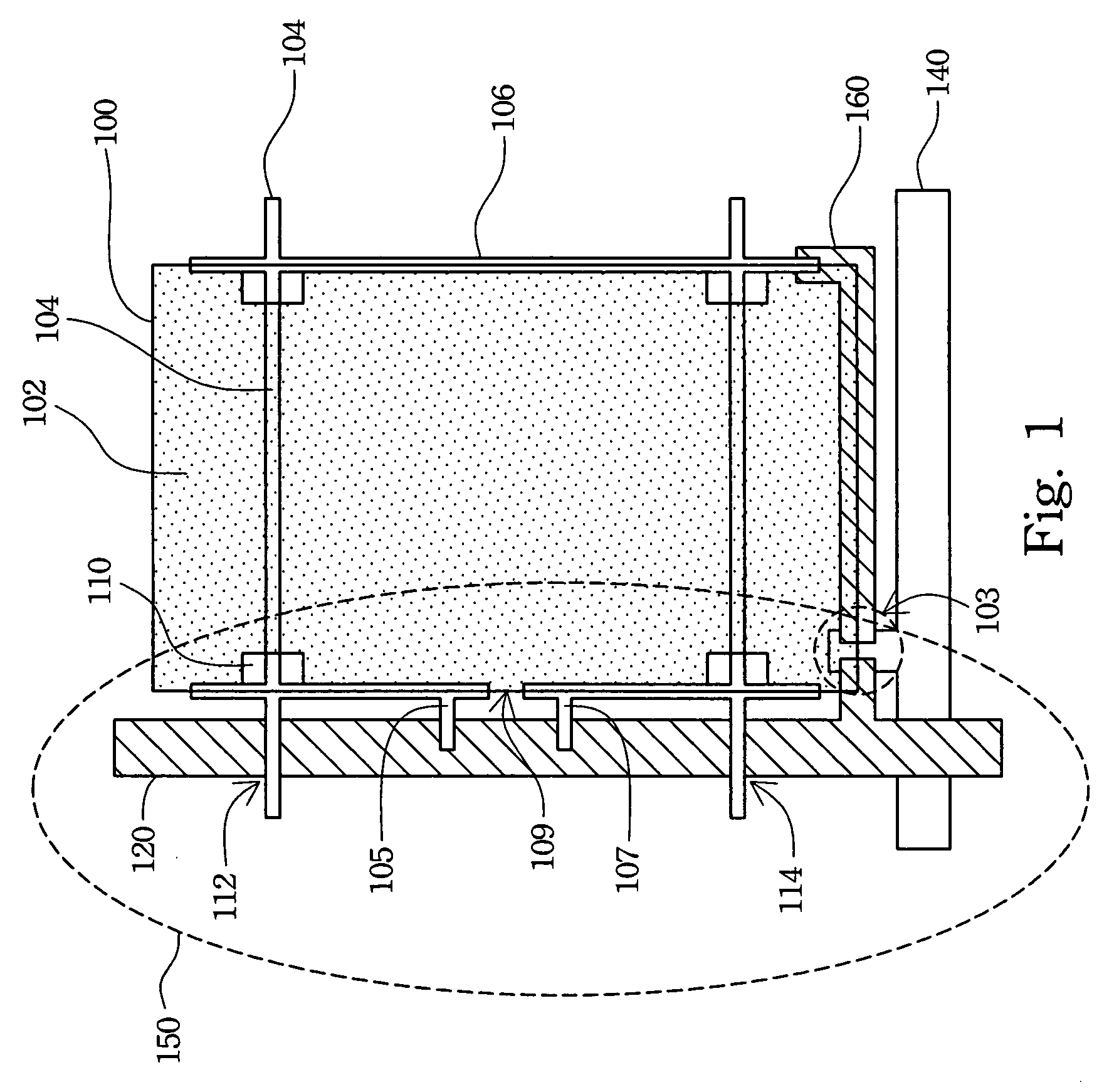
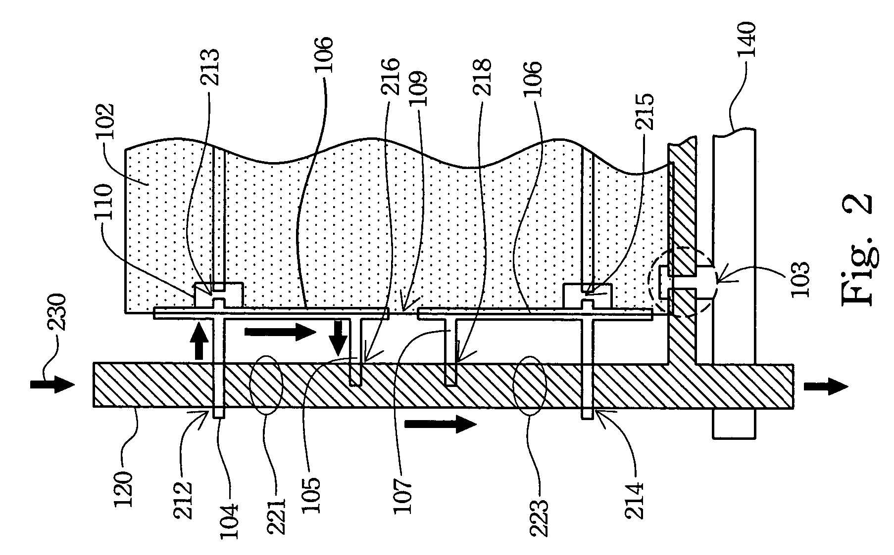
[0022] The present invention discloses a liquid crystal display (LCD) with defect reparability. Referring to FIG. 1 and FIG. 2 respectively, FIG. 1 is a top view showing a partial structure of the LCD in accordance with the first preferred embodiment of the present invention, and FIG. 2 is a schematic diagram showing the defect repair of the LCD in accordance with the first preferred embodiment of the present invention. The position shown in FIG. 2 is an enlarged view of the region 150 in FIG. 1.
[0023] In FIG. 1, a region 100 cross-controlled by a data line 120 and a scan line 140 respectively is a pixel display area covered by a pixel electrode 102. The display state of the display region 100 is controlled by the thin film transistor (TFT) 103, and a signal from the data line 120 is transmitted to the region 100 by a drain metal 160 contacting to the pixel electrode 102. For the display region 100 with a Cst-on-common design, two horizontal common lines 104 and two vertical common...
embodiment 2
[0040] The present invention discloses another LCD with defect-reparability. The pattern of the horizontal common lines is changed to reduce leakage of light from the openings designed in the pixel electrode. Referring to FIG. 4, a top view is shown of a partial structure of the LCD in accordance with the second preferred embodiment of the present invention.
[0041] In FIG. 4, two horizontal common lines 404 and two vertical common lines 406 are placed in the region 400 which is cross-controlled by a data line 420 and a scan line 440, and each horizontal common line 404 is connected with each vertical common line 406. The horizontal common lines 404 are located between the vertical common lines 406, but are not extended to the data line 420 as they are in the first embodiment; the data line 420 also has no overlaps with the horizontal common lines 404. Moreover, each horizontal common line 404 is designed as an oblique line such that horizontal common lines 404 are unparallel.
[0042]...
embodiment 3
[0047] The present invention discloses further a LCD with defect reparability. Defect reparability is obtained by using the common lines, and Cst is also made adjustable by utilizing a geometry change of the common lines in the third embodiment.
[0048] Referring to FIG. 5, a top view is shown of a partial structure of the LCD in accordance with the third preferred embodiment of the present invention. In FIG. 5, two horizontal common lines 504 and two vertical common lines 506 are placed in the a pixel display region 500 cross-controlled by a data line 520 and a scan line 540, and each horizontal common line 504 is connected with each vertical common line 506. The horizontal common lines 504 are located between the vertical common lines 506, but unlike the first embodiment, the horizontal common lines 504 are not extended to the data line 520 and have no overlaps with the data line 520. Compared with the second embodiment, each horizontal common line 504 is designed as a zigzag patte...
PUM
 Abstract
Description
Claims
Application Information