
A system and method of providing error detection and correction capability in an integrated circuit using redundant logic cells of an embedded FPGA

a technology of applied in the field of system and method of providing error detection and correction capability in integrated circuit (ic), can solve problems such as not designed to fix logic structure or logic errors

Active Publication Date: 2005-12-15
MARVELL ASIA PTE LTD
View PDF12 Cites 20 Cited by
  • Summary
  • Abstract
  • Description
  • Claims
  • Application Information

AI Technical Summary

Benefits of technology

The present invention provides a new way to fix logic functions in an IC design. It allows data signals to be routed to a defective logic function through embedded FPGA structures and a corrected logic function in another area of the IC design. The output of the corrected function is then routed back to the defective function's return cone of logic. This creates a logic EC (embedded FPGA) within the IC chip. The invention can be used during product design and development or as a program logic fix. It also has application in evaluating error recovery of an IC chip design, where data errors can be injected through the embedded FPGA structures, and the logic function IC design is evaluated as to how well it handles error recovery. The invention is applicable to any standard IC cell design with embedded FPGA structures.

Problems solved by technology

One limitation of current ICE structures is that they are not designed to fix logic structures or logic errors within the design of a microprocessor IC.

Method used


Image

  • A system and method of providing error detection and correction capability in an integrated circuit using redundant logic cells of an embedded FPGA
  • A system and method of providing error detection and correction capability in an integrated circuit using redundant logic cells of an embedded FPGA
  • A system and method of providing error detection and correction capability in an integrated circuit using redundant logic cells of an embedded FPGA

Examples


Embodiment Construction

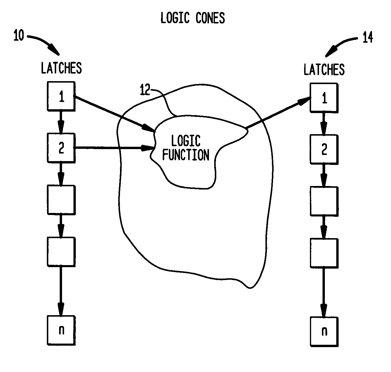
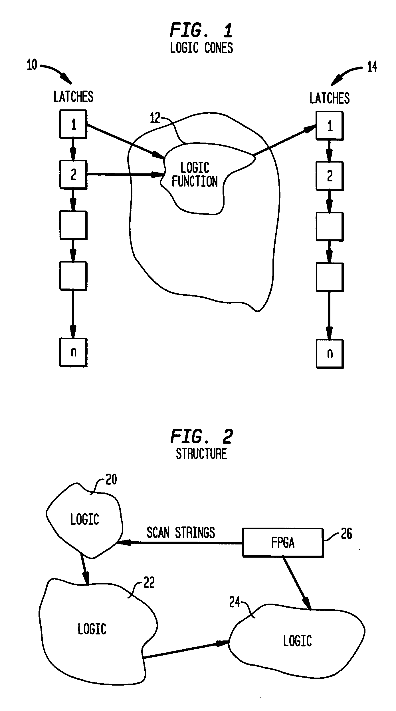
[0014]FIG. 1 illustrates the general concept of cones of logic existing in association with a logic function bounded by latches. A set of latches 1, 2 . . . n in a scan string 10 on the left form inputs to a logic function 12, which forms inputs to a set of latches 1, 2 . . . n in a scan string 14 on the right, forming an input cone of logic on the left and an output cone of logic on the right. The logic function 12 can be a logic cell, logic book, or any logic function typically comprised of AND, OR, NOR and other logic gates arranged to accomplish some logic function, such as to execute a truth table. The cone of logic can be traced upstream from the logic function 12 to determine all input latches to the logic function 12, and the cone of logic can be traced downstream from the logic function 12 to determine all output latches from the logic function 12. The logic function 12 is typically tested by scanning in a data test pattern from the input latches into the logic function, an...


PUM


Abstract

A system and method of providing error detection and correction capability in an IC using redundant logic cells and an embedded field programmable gate array (FPGA). The system and method provide error correction (EC) to enable a defective logic function implemented within an IC chip design to be replaced, wherein at least one embedded FPGA is provided in the IC chip to perform a logic function. If a defective logic function is identified in the IC design, the embedded FPGA is programmed to correctly perform the defective logic function. All inputs in an input cone of logic of the defective logic function are identified and are directed into the embedded FPGA, such that the embedded FPGA performs the logic function of the defective logic function. All outputs in an output cone of logic of the defective logic function are identified, and the output of the FPGA is directed to the output cone of logic of the defective logic function, such that logic EC is provided within the embedded FPGA structure of the IC chip.

Description

BACKGROUND OF INVENTION [0001] 1. Field of the Invention [0002] The present invention relates generally to a system and method of providing error detection and correction capability in an integrated circuit (IC) using redundant logic cells and an embedded field programmable gate array (FPGA). The embedded FPGA provides for in circuit emulator (ICE) breakpoint and logic error correction (EC). The present invention provides flexible embedded logic engineering changes within the IC chip without requiring the contents of the latches of the logic function to be scanned to an external boundary, to make an EC change externally. [0003] The EC method of the present invention can be used either during product design and development, or as a logic fix post-silicon fabrication. The subject invention also has application in evaluating error recovery of an IC chip design, wherein data errors can be injected through the embedded FPGA structures, and then the logic function IC design is evaluated a...

Claims


Application Information

Patent Timeline
Patent Type & Authority Applications(United States)
IPC IPC(8): G06F11/00
CPCG01R31/318519H03K19/00392G06F11/261G01R31/318558
Inventor COHN, JOHN M.REYNOLDS, CHRISTOPHER B.VENTRONE, SEBASTIAN T.ZUCHOWSKI, PAUL S.
Owner MARVELL ASIA PTE LTD
Learn More