System and method for testing and configuring semiconductor functional circuits

a functional circuit and semiconductor technology, applied in the field of semiconductor manufacturing, can solve the problems of high cost, resource intensive activity, complex manufacturing process for building integrated circuits, and difficult design and building of integrated circuits with diverse functional and performance characteristics, and achieve the effect of facilitating user interaction and facilitating user interaction

Active Publication Date: 2005-12-15
NVIDIA CORP
View PDF99 Cites 36 Cited by
  • Summary
  • Abstract
  • Description
  • Claims
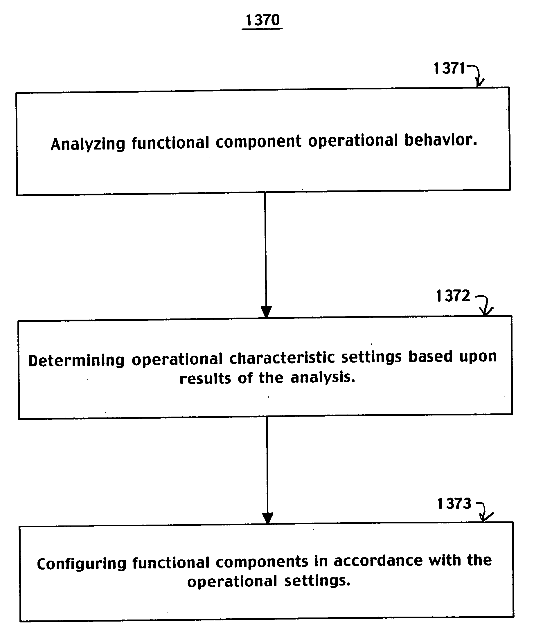
  • Application Information

AI Technical Summary

Benefits of technology

[0009] Functional component configuration related information can be presented in a variety of convenient formats including a graphical user interface (GUI). In one embodiment, the GUI indicates a pass or fail status for functional component building blocks at various levels of granularity and in real time. The graphical user interface can present topological inversion information in a user friendly manner that are otherwise dispersed in an imperfect Cartesian order. The graphical user interface can also facilitate user interaction with various functional component operational behavior analyzing features and operational characteristics settings determining features. For example, the graphical user interface can facilitate user interaction in failing pattern recognition, production test tuning and field configuration algorithm adjustment.

Problems solved by technology

However, designing and building integrated circuits with diverse functionality and performance characteristics is challenging.
Additionally, the manufacturing process to build the integrated circuits is highly complex and resource intensive.
Manufacturing integrated circuits is an expensive, resource intensive activity, in which numerous computational components are included in a single integrated circuit unit.
However, providing appropriate and efficient functionality at acceptable reliability is often difficult.
Yields for wafers with high performance die with a large number of components can be very low.
This approach usually results in considerable waste of precious die area and resources on fabricating components that remain “surplus” even after replacing defective components.
Such surplus components do not contribute to functionality and / or operational productivity.
In addition, the end result is a usable integrated circuit with limited capability and that does not provide a full range of functionality (e.g., not able to perform floating point operations).
Traditionally, the integrated circuits with the defective functional components would otherwise be discarded resulting in the costs of producing a wafer being assigned to fewer acceptable die.

Method used


Image

  • System and method for testing and configuring semiconductor functional circuits
  • System and method for testing and configuring semiconductor functional circuits
  • System and method for testing and configuring semiconductor functional circuits

Examples


Embodiment Construction

[0033] Reference will now be made in detail to the preferred embodiments of the invention, examples of which are illustrated in the accompanying drawings. While the invention will be described in conjunction with the preferred embodiments, it will be understood that they are not intended to limit the invention to these embodiments. On the contrary, the invention is intended to cover alternatives, modifications and equivalents, which may be included within the spirit and scope of the invention as defined by the appended claims. Furthermore, in the following detailed description of the present invention, numerous specific details are set forth in order to provide a thorough understanding of the present invention. However, it will be obvious to one of ordinary skill in the art that the present invention may be practiced without these specific details. In other instances, well known methods, procedures, components, and circuits have not been described in detail as not to unnecessarily o...


PUM


Abstract

The present invention systems and methods enable configuration of functional components in integrated circuits. A present invention system and method can flexibly change the operational characteristics of functional components in an integrated circuit die based upon a variety of factors including manufacturing defects, compatibility characteristics, performance requirements, and system health (e.g., the number of components operating properly). Functional component operational behavior is tested and analyzed at various levels of configuration abstraction and component organization (e.g., topological inversion analysis). The testing and analysis can be performed in parallel on numerous functional components. Functional component configuration related information is presented in a graphical user interface (GUI) at various levels of granularity and in real time. The graphical user interface can facilitate user interaction in recognizing failure patterns, production test tuning and field configuration algorithm adjustment. The testing and analysis information can also be organized in a variety of convenient database formats.

Description

RELATED APPLICATIONS [0001] This application claims the benefit of co-pending commonly-owned U.S. Patent Provisional Application Ser. No. 60 / 503,710 (attorney docket number NVID P000871.PRO), filed Sep. 15, 2003, entitled “A SYSTEM AND METHOD FOR CONFIGURING SEMICONDUCTOR FUNCTIONAL COMPONENTS” which is hereby incorporated by this reference. This application is a continuation-in-part and claims the benefit of co-pending commonly-owned U.S. patent application Ser. No. 10 / 740,722 (attorney docket number NVID P000784), filed Dec. 18, 2003, entitled “A SYSTEM AND METHOD FOR TESTING AND CONFIGURING SEMICONDUCTOR FUNCTIONAL CIRCUITS” which is hereby incorporated by this reference. This application is a continuation-in-part and claims the benefit of co-pending commonly-owned U.S. patent application Ser. No. 10 / 740,779 (attorney docket number NVID P001161), filed Dec. 18, 2003, entitled “A SYSTEM AND METHOD FOR REMOTELY CONFIGURING SEMICONDUCTOR FUNCTIONAL CIRCUITS” which is hereby incorpor...

Claims


Application Information

Patent Timeline
Patent Type & Authority Applications(United States)
IPC IPC(8): G06F11/00G06F17/50G06F19/00
CPCG01R31/31704G01R31/3185G06F11/267G06F11/27H01L2924/0002H01L22/22H01L2924/00
Inventor DIAMOND, MICHAEL B.
Owner NVIDIA CORP
Why Eureka
Try Eureka