MEMS structure and method for fabricating the same

Inactive Publication Date: 2005-12-22
SAMSUNG ELECTRO MECHANICS CO LTD
View PDF1 Cites 31 Cited by
  • Summary
  • Abstract
  • Description
  • Claims
  • Application Information

AI Technical Summary

Benefits of technology

[0020] Therefore, the present invention has been made in view of the above problems, and it is an object of the present invention to provide a MEMS structure which is capable of preventing electrical short circuit even

Problems solved by technology

This is called “stiction” which interferes with driving of the MEMS structure 1, thus greatly deteriorating characteristics of the products.
Further, where it is severe, there is difficulty in manufacturing the device, presenting a factor of decreasing yield of the micromachining process.
However, the conventional methods to prevent the stiction phenomenon from occurring in the MEMS structure 1 have disadvantages such as decreased yield, additional steps in a manufacturing process and expensive equipment.
Further, under the condition in which opposite electrical polarities are applied to the movable portion

Method used


Image

  • MEMS structure and method for fabricating the same
  • MEMS structure and method for fabricating the same
  • MEMS structure and method for fabricating the same

Examples


Embodiment Construction

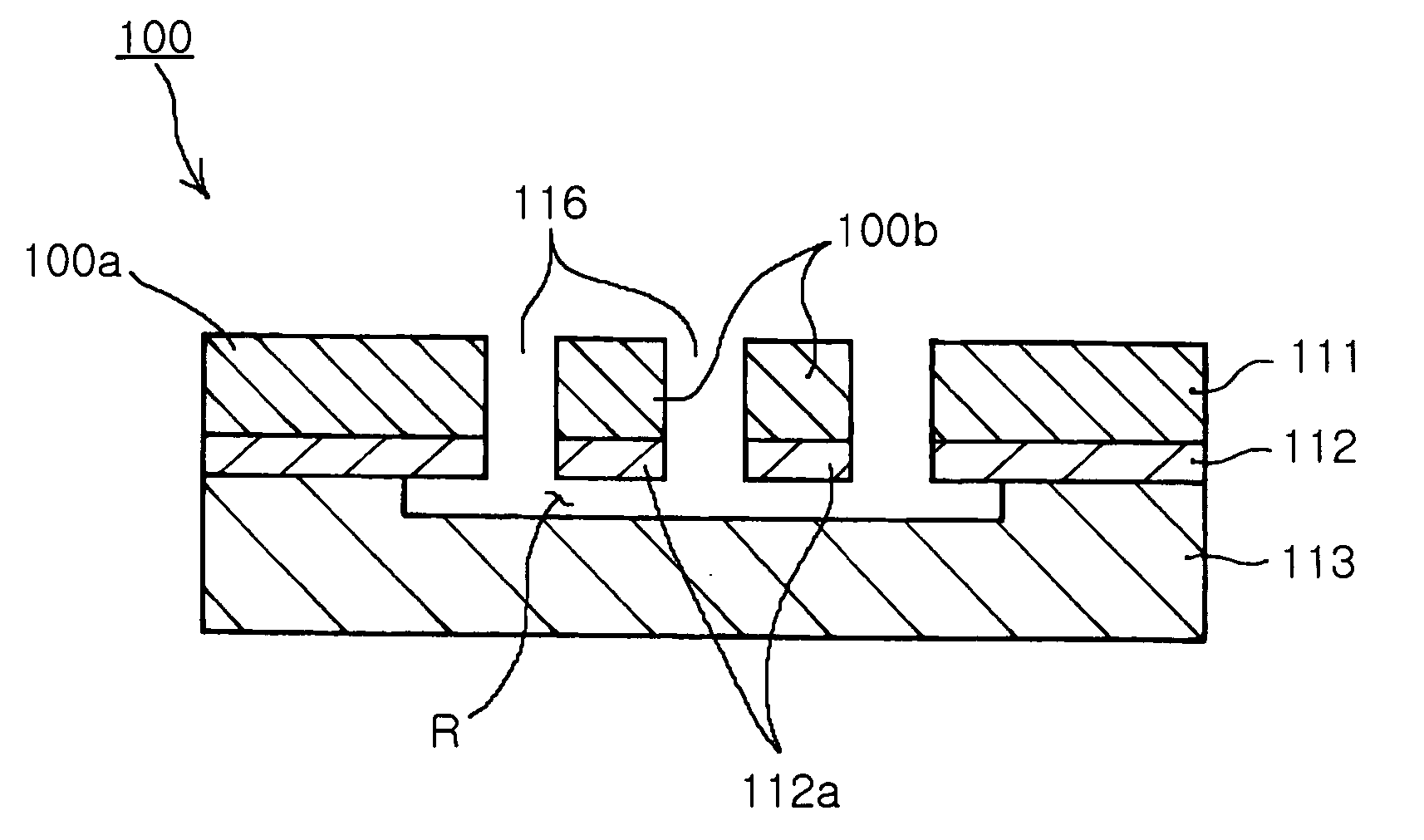
[0046] Preferred embodiments of the present invention will now be described in detail with reference to the annexed drawings. FIGS. 3a through 3f illustrate the steps for fabricating a MEMS structure in accordance with the present invention. FIG. 4 shows a cross-sectional view of a MEMS structure in accordance with the present invention.

[0047] Referring to FIGS. 3 and 4, a MEMS structure 100 of the present invention includes a stationary portion 100a integrally formed on a wafer substrate 110, and a movable portion 100b movably formed relative to the stationary portion 100a. The MEMS structure in accordance with the present invention may fundamentally prevent a stiction phenomenon occurring during the drying process of the etchant used in the wet etching process by forming the movable portion 100b and a floating space R for floating the movable portion 100b by the dry etching process.

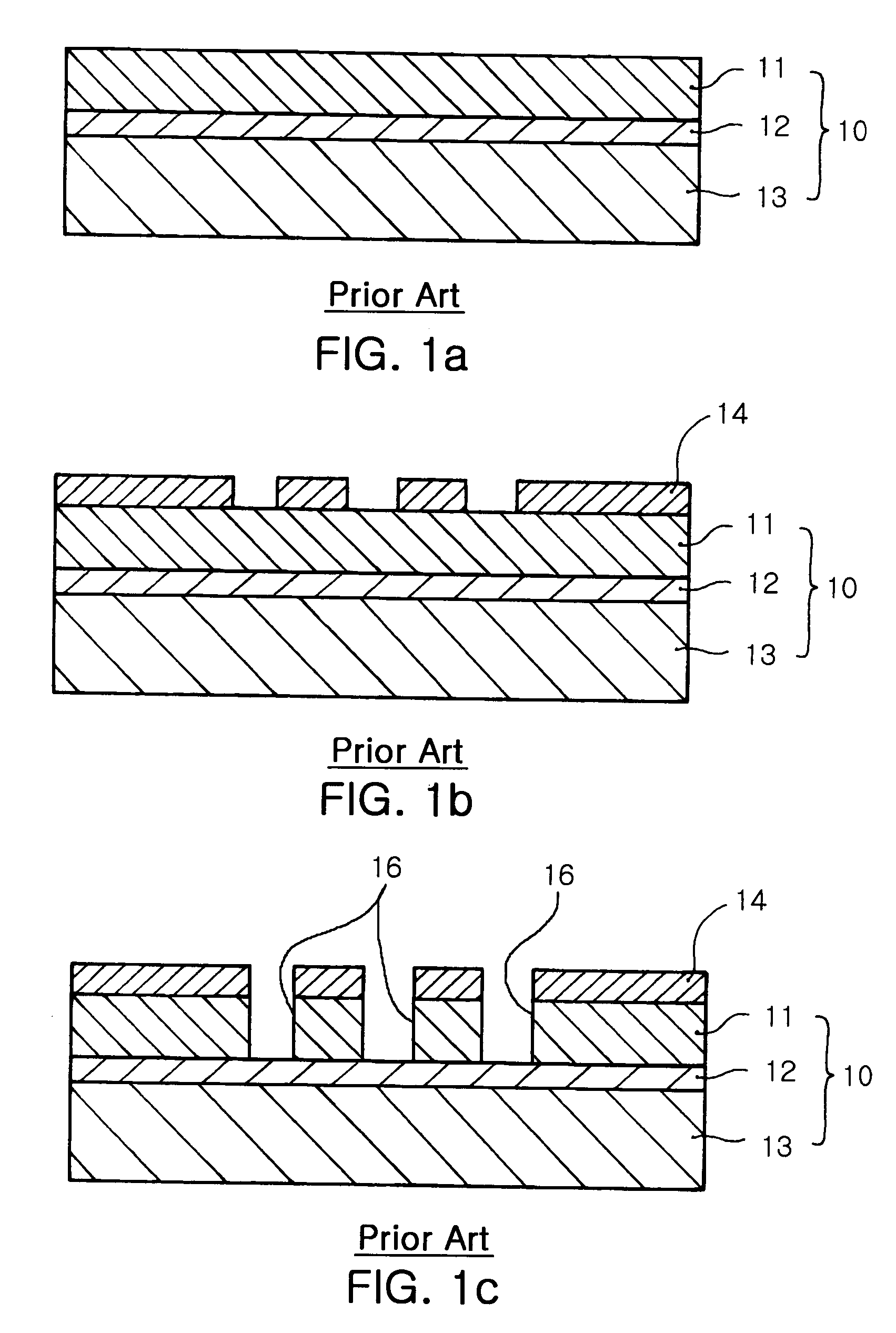
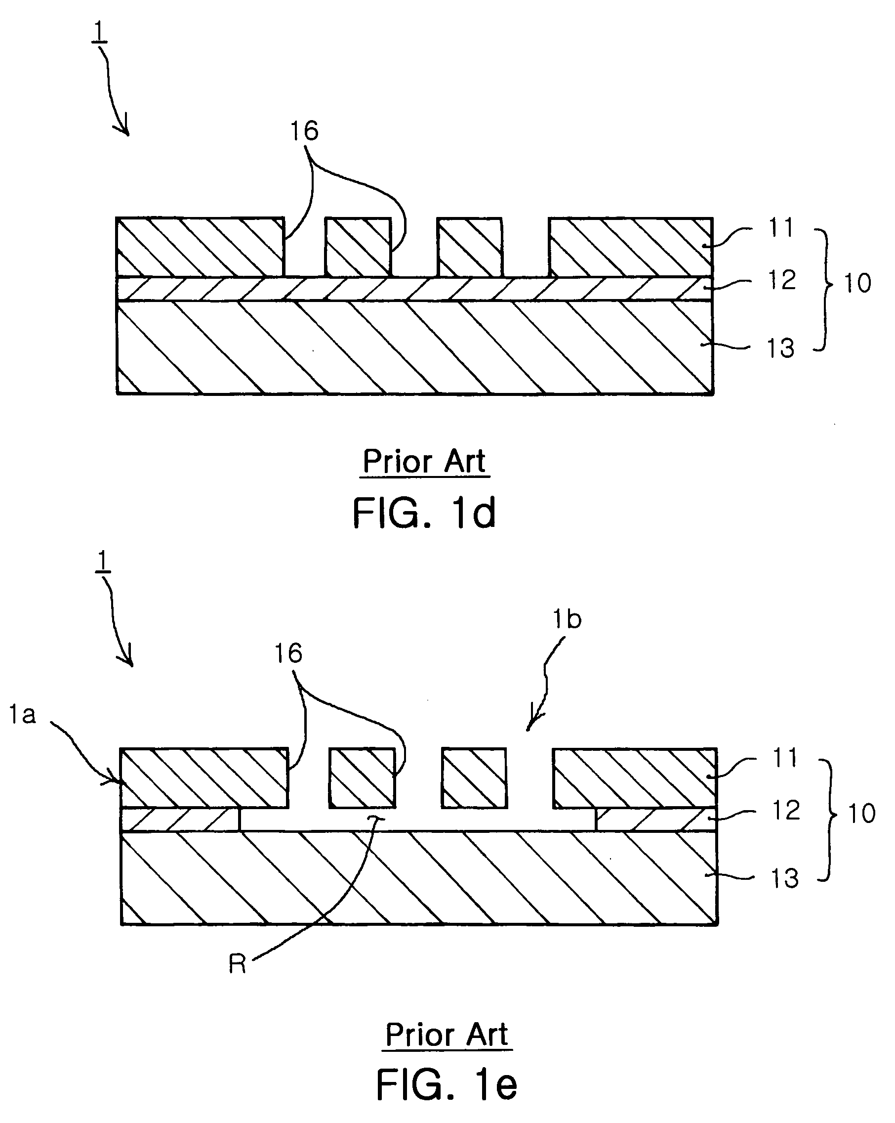
[0048] As shown in FIG. 3a, there is provided the wafer substrate 110 in which a predetermined thi...


PUM

PropertyMeasurementUnit
Thicknessaaaaaaaaaa
Electric potential / voltageaaaaaaaaaa
Depthaaaaaaaaaa

Abstract

A MEMS structure includes a floating space formed on the upper silicon layer by a first dry etching, and then dry etched to a predeterminded depth on the lower silicon layer by etching gas supplied through the etched holes from which the oxide film has been removed at the bottom surface thereof in a second dry etching process, so as to float the movable portion; and the oxide film for preventing electrical short circuit remaining on the lower surface of the movable portion so as to correspond to the lower silicon layer leaving the floating space therebetween.

Description

BACKGROUND OF THE INVENTION [0001] 1. Field of the Invention [0002] The present invention relates to a MEMS structure and a method for fabricating the same, and more particularly to a MEMS structure in which a floating space for allowing a movable portion to move is formed by a dry etching process, and thus is capable of fundamentally preventing a stiction phenomenon which occurs when drying an etchant or other liquid, securing electrical properties and stability thereof, and preemptively preventing electrical short circuit due to stiction; and a method for fabricating the same. [0003] 2. Description of the Related Art [0004] Recently, a number of products employing Micro-Electro Mechanical Systems (MEMS) technology which is advantageous for miniaturization and high accuracy has been developed. To this MEMS technology are applied various techniques for fabricating a MEMS structure having a stationary portion fixed in a position by a variety of methods, and a movable portion moving r...

Claims


Application Information

Patent Timeline
IPC IPC(8): B81B7/02B81C1/00H01L21/00H01L27/14
CPCB81C2201/0132B81C1/00936B81B7/02
Inventor KIM, JONG SAMLEE, SUNG JUNLEE, RO WOON
Owner SAMSUNG ELECTRO MECHANICS CO LTD
Why Eureka
Try Eureka