Flip-flop circuit

a flip-flop circuit and circuit technology, applied in the field of flip-flop circuits, can solve the problems of difficult design and development of circuits including such flip-flop circuits, difficult to extract physical characteristics that are to be registered in a library as those of standard cells, and processing becomes very complicated, so as to achieve the effect of easy holding and outpu

Inactive Publication Date: 2005-12-22
PANASONIC CORP
View PDF4 Cites 33 Cited by
  • Summary
  • Abstract
  • Description
  • Claims
  • Application Information

AI Technical Summary

Benefits of technology

[0020] If a tri-state inverter or an inverter is used as the tri-state element or the driver descr...

Problems solved by technology

Therefore, the flip-flop circuit has a drawback in which it is difficult to design and develop a circuit including such a flip-flop circuit in a short period.
However, in the case where physical characteristics at the input and output vary depending on the state of a clock signal as described above, it is difficult to extract physical characteristics that are to be registered in a library as those of standard cells.
If physical characteristics associated with the respect...

Method used


Image

  • Flip-flop circuit
  • Flip-flop circuit
  • Flip-flop circuit

Examples


embodiment 1

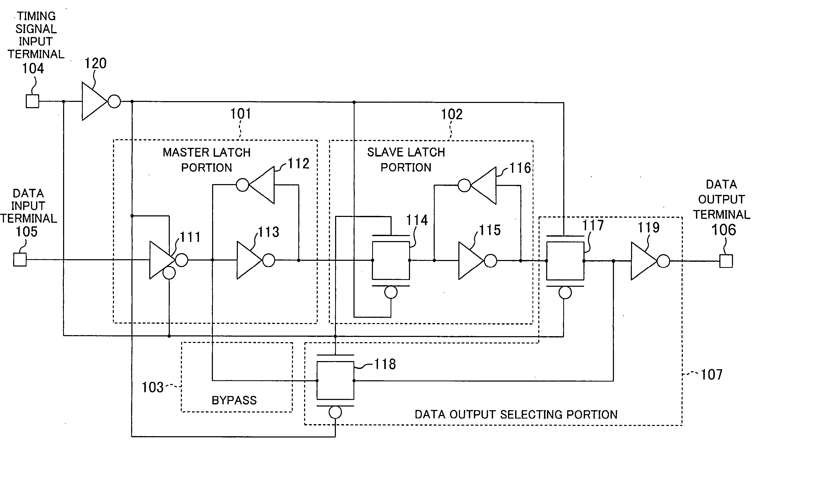
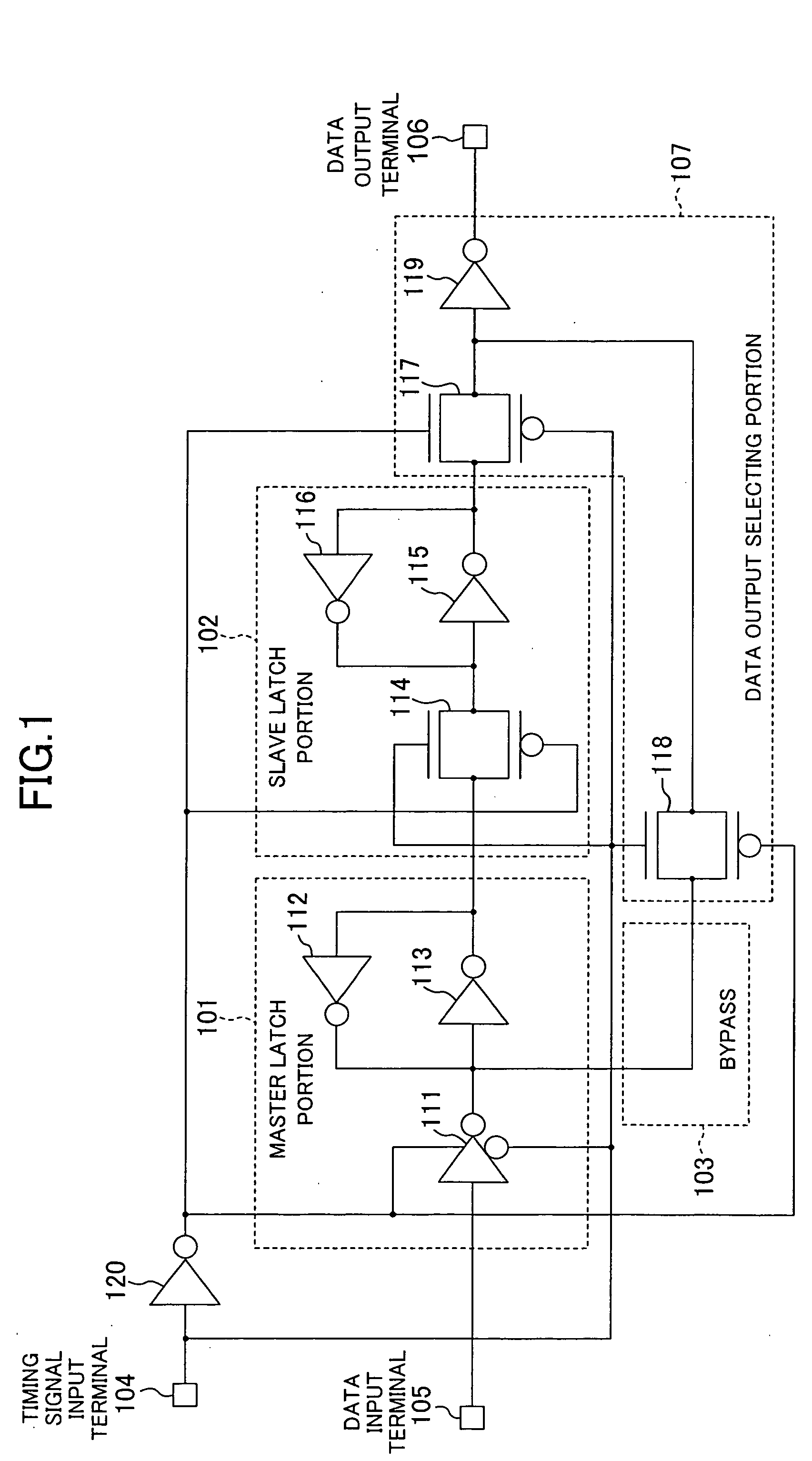
[0030]FIG. 1 is a circuit diagram illustrating a flip-flop circuit according to a first embodiment of the present invention.

[0031] A master latch portion 101 includes: a tri-state inverter 111; an inverter 112; and an inverter 113. The master latch portion 101 performs latch operation for allowing data to be written therein when a timing signal input from a timing signal input terminal 104 is “0” (e.g., at an L level) and holding data when the timing signal is “1” (e.g., at an H level). The inverter 112 has a driving capability lower than that of the tri-state inverter 111.

[0032] A slave latch portion 102 includes: a pass gate 114; an inverter 115; and an inverter 116. The slave latch portion 102 holds data when the timing signal is “0” and allows data to be written therein when the timing signal is “1”. The inverter 116 has a driving capability lower than that of the tri-state inverter 113 connected thereto via the pass gate 114.

[0033] A bypass 103 is a signal line for outputtin...

embodiment 2

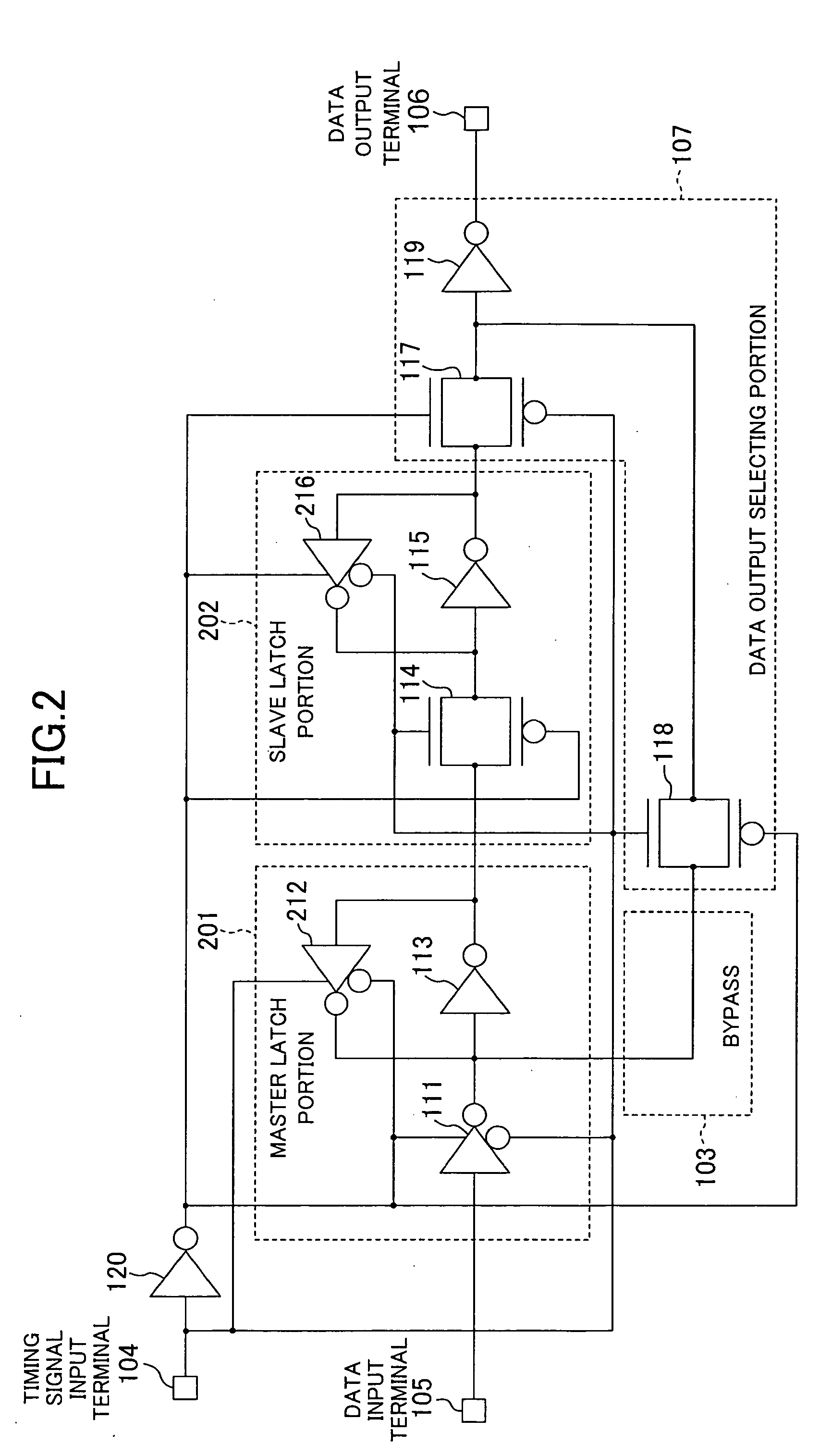
[0047] Instead of the master latch portion 101 and the slave latch portion 102 including the inverters 112 and 116, respectively, of the first embodiment, a master latch portion 201 and a slave latch portion 202 including tri-state inverters 212 and 216, respectively, may be used as shown in FIG. 2.

[0048] The tri-state inverters 212 and a tri-state inverter 111 operate at different states of a timing signal, and the tri-state inverter 216 and a pass gate 114 also operate at different states of the timing signal. Accordingly, the outputs of the tri-state inverter 212 and the tri-state inverter 111 do not conflict with each other, and the outputs of the tri-state inverter 216 and the pass gate 114 do not conflict with each other.

[0049] With this configuration, holding operation of input data itself is also the same as that in the conventional flip-flop circuit, as described in the first embodiment.

[0050] In addition, irrespective of the state of the timing signal, only the gate ter...

embodiment 3

[0051] Instead of the data output selecting portion 107 of the first embodiment, a data output selecting portion 307 including tri-state inverters 317 and 318 may be provided as shown in FIG. 3. When the value of a timing signal is “0”, the tri-state inverters 317 and 318 select the output of a slave latch portion 102 (i.e., the tri-state inverter 317 is active and the tri-state inverter 318 is in a high-impedance state). On the other hand, when the value of the timing signal is “1”, the tri-state inverters 317 and 318 select the output from a bypass 103 (i.e., the tri-state inverter 317 is in a high-impedance state and the tri-state inverter 318 is active).

[0052] In this embodiment, the tri-state inverters 317 and 318 have the same driving capability (physical characteristic). Specifically, elements (transistors) constituting these inverters are designed to have the same size and shape, for example. That is, the driving capability of the tri-state inverter 317 does not affect the ...


PUM


Abstract

To keep input capacitance and driving capability at respective data input and output terminals of a flip-flop circuit, the flip-flop includes: a mater latch portion; a slave latch portion; and a data output selecting portion. The master latch portion includes a tri-state inverter, which is connected to the input terminal. The data output selecting portion is constituted by two pass gates and an inverter, which is connected to the output terminal. The input capacitance of the flip-flop circuit is determined by gate capacitances of transistors constituting the tri-state inverter connected to the input terminal. The driving capability of the flip-flop circuit is determined by the driving capability of the inverter connected to the output terminal. Accordingly, both the input capacitance and the driving capability are kept constant, irrespective of the state of a timing signal such as a clock signal.

Description

CROSS-REFERENCE TO RELATED APPLICATION [0001] This Nonprovisional application claims priority under 35 U.S.C. §119 (a) on Patent Application No. 2004-179954 filed in Japan on Jun. 17, 2004, the entire contents of which are hereby incorporated by reference. BACKGROUND OF THE INVENTION [0002] The present invention mainly relates to flip-flop circuits constituted by transistors formed as semiconductor integrated circuits (LSIs). [0003] Performances required of recent LSIs have been rapidly enhanced in recent years, and LSI manufacturers have competed to achieve higher functionality and higher operation speed. LSI circuits for use in synchronous digital signal processing, for example, are designed to use flip-flop circuits as necessary components. Therefore, to achieve faster LSI circuits, every manufacturer has to increase the speed of flip-flop circuits. [0004] In view of this, various configurations of flip-flop circuits for high speed operation have been proposed to date. For exampl...

Claims


Application Information

Patent Timeline
IPC IPC(8): H03K3/00H03K3/011H03K3/012H03K3/037H03K3/3562H03K5/12
CPCH03K3/011H03K3/35625H03K3/0372H03K3/012
Inventor INOUE, GENICHIRO
Owner PANASONIC CORP
Why Eureka
Try Eureka