Substrate processing unit and substrate processing apparatus

a processing unit and substrate technology, applied in the direction of pile separation, transportation and packaging, liquid/solution decomposition chemical coating, etc., can solve the problems of increasing the cost reducing the processing efficiency of the clean room, and complicated process control between the processes, so as to reduce the space and reduce the energy needed for substrate transportation

Active Publication Date: 2005-12-22
EBARA CORP
View PDF12 Cites 13 Cited by
  • Summary
  • Abstract
  • Description
  • Claims
  • Application Information

AI Technical Summary

Benefits of technology

[0017] The present invention has been made in view of the above situation in the related art. It is therefore a first object of the present invention to provide a substrate processing unit and a substrate processing apparatus which, by employing the processing unit to carry out different processings with different processing liquids, can make a reduction in the space for carrying out the entire process of substrate processing and a reduction in the energy necessary for substrate transportation.

Problems solved by technology

As a result, not only the throughput is lowered, but also process control between the processes is complicated.
Furthermore, the apparatus has an increased size and occupies the wide installation space in the clean room, leading to the increased cost of the clean room.
This is because though the use of a single processing unit to carry out different processings with different processing liquids can reduce the space for carrying out the entire process of substrate processing and can also reduce the energy necessary for substrate transportation, it is difficult to avoid mixing or dilution of different processing liquids when a single processing unit is employed for carrying out different processings using the different processing liquids.
In some cases, however, a substrate strongly sticking to an attracting seal, such as a rubber, cannot be released only by the introduction of clean gas, such as N2 gas.
However, when employing the method involving simultaneous jetting of clean gas and pure water e.g. in a substrate holding apparatus adapted for the vacuum attraction method, two circuits for the introductions of a clean gas and of pure water are necessary in addition to a circuit for vacuuming, leading to a complicated circuit construction and an increased size of apparatus.
There are, therefore, cases in which a load is applied locally on a substrate to cause deformation, or a substrate strongly sticks to e.g. an attracting seal whereby release of the substrate becomes difficult.

Method used


Image

  • Substrate processing unit and substrate processing apparatus
  • Substrate processing unit and substrate processing apparatus
  • Substrate processing unit and substrate processing apparatus

Examples


Embodiment Construction

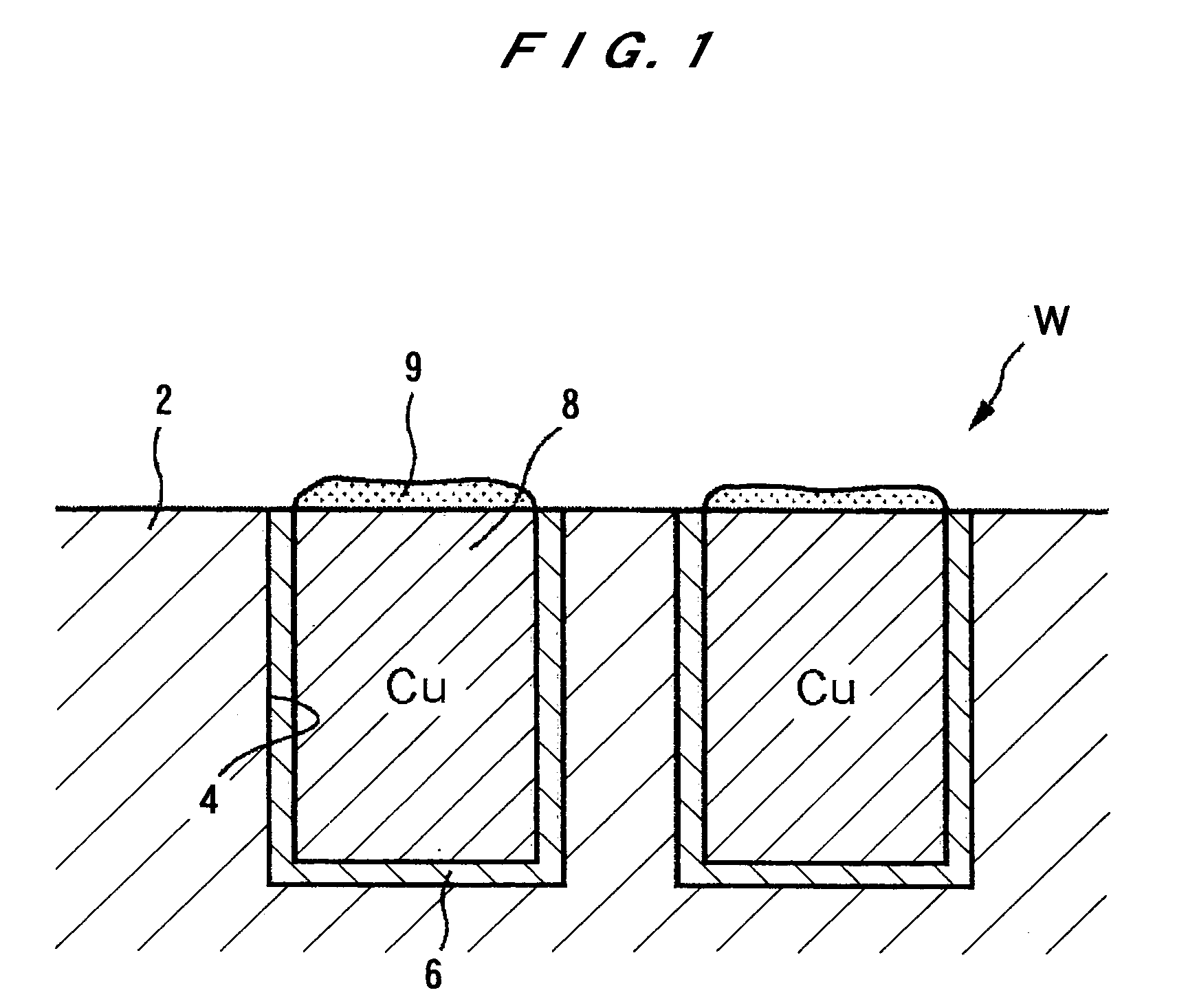
[0080] Preferred embodiments of the present invention will now be described with reference to the drawings. The following description illustrates the case of applying the present invention to an electroless plating apparatus adapted to efficiently form a protective film 9 (see FIG. 1) by electroless plating on surfaces of interconnects formed on a substrate. The present invention is, of course, applicable to other substrate processing apparatuses, such as an electroplating apparatus, a CVD apparatus, and the like.

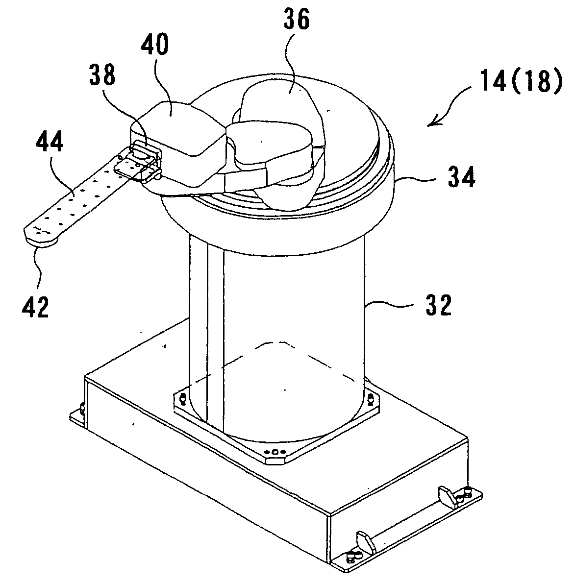
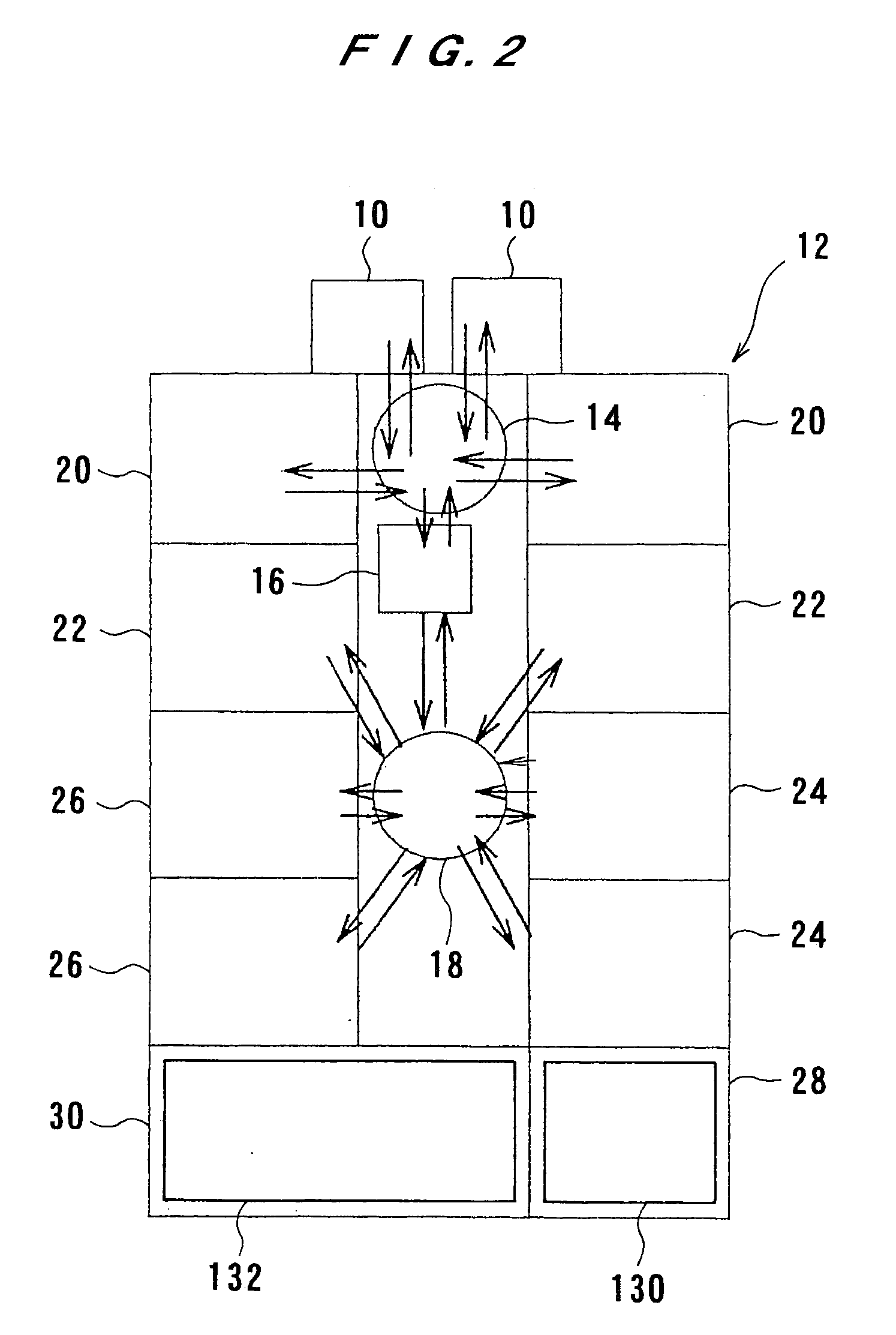
[0081]FIG. 2 shows a layout plan view of a substrate processing apparatus (electroless plating apparatus) according to an embodiment of the present invention. As shown in FIG. 2, the substrate processing apparatus includes a rectangular apparatus frame 12, and a transport box 10, such as a SMIF box, detachably mounted to the apparatus frame 12 and housing therein a number of substrates such as semiconductor wafers. Located centrally in the apparatus frame 12, there are dis...


PUM

PropertyMeasurementUnit
temperatureaaaaaaaaaa
chemicalaaaaaaaaaa

Abstract

A substrate processing unit, by employing the processing unit to carry out different processings with different processing liquids, can make a reduction in the space for carrying out the entire process of substrate processing and a reduction in the energy necessary for substrate transportation. The substrate processing unit includes: a vertically-movable substrate holder for holding a substrate; an pan surrounding the periphery of the substrate holder; an cell, located below the substrate holder and within the pan, having in its interior a chemical processing section; and a cell cover, capable of closing the top opening of the cell, having a plurality of spray nozzles for separately spraying at least two types of processing liquids; wherein the pan and the cell each have an individual liquid discharge line.

Description

BACKGROUND OF THE INVENTION [0001] 1. Field of the Invention [0002] The present invention relates to a substrate processing unit and a substrate processing apparatus, and more particularly to a substrate processing unit and a substrate processing apparatus which are useful for forming a protective film, for example, by electroless plating, on exposed surfaces of embedded interconnects of a conductive material (interconnect material), such as copper or silver, embedded in fine interconnect recesses provided in a surface of a substrate, such as a semiconductor wafer. [0003] The present invention also relates to a substrate holding apparatus and a substrate holding method which can be advantageously used in processing a surface (processing surface) of a substrate with a plating solution or other processing liquid. [0004] 2. Description of the Related Art [0005] As a process for forming interconnects in a semiconductor device, a so-called “damascene process”, which comprises embedding a...

Claims


Application Information

Patent Timeline
Patent Type & Authority Applications(United States)
IPC IPC(8): B05B15/12B05C3/09B05C9/06B05C11/10B05C13/00B05C15/00B05D3/12B65H1/00C23C2/00C23C18/16C23C18/31C25D17/06H01L21/00H01L21/288H01L21/68H01L21/683H01L21/768
CPCC23C2/003C23C18/1619C23C18/163C23C18/1642H01L21/76849H01L21/6708H01L21/67742H01L21/6838H01L21/288H01L21/02H01L21/304
Inventor KATSUOKA, SEIJISEKIMOTO, MASAHIKOWATANABE, TERUYUKIKATO, RYOYOKOYAMA, TOSHIOSUZUKI, KENICHIKOBAYASHI, KENICHI
Owner EBARA CORP
Why Eureka
Try Eureka