Atomic layer deposition for filling a gap between devices

a technology of atomic layer and gap, which is applied in the direction of semiconductor/solid-state device manufacturing, basic electric elements, electric devices, etc., can solve the problems of contact leakage or a more serious short circuit, the inability to achieve and the difficulty of small lateral dimensions and precise dimensional control

Inactive Publication Date: 2005-12-22
TAIWAN SEMICON MFG CO LTD
View PDF8 Cites 225 Cited by
  • Summary
  • Abstract
  • Description
  • Claims
  • Application Information

AI Technical Summary

Problems solved by technology

As the material is deposited, growth progresses laterally as well as vertically making achievement of small lateral dimensions and precise dimensional control more difficult.
Trapped voids are undesirable.
The void 150 may result in contact leakage or a more serious short circuit.
For example, poor gap fill on the interlayer dielectric leads to tungsten stringers, which can result in a contact short.
Non-linear bias may also result.
The prior art deposition of PSG by HDP CVD has its limitations for gap fill between devices.
Generally, this process cannot be used for filling gaps with a spacing X less than 350 angstroms, without the likelihood of void formation.
In more advanced technologies with smaller geometries, even SA CVD may not be an adequate solution for filling the gap between devices.

Method used


Image

  • Atomic layer deposition for filling a gap between devices
  • Atomic layer deposition for filling a gap between devices
  • Atomic layer deposition for filling a gap between devices

Examples


Embodiment Construction

[0015] This description of the exemplary embodiments is intended to be read in connection with the accompanying drawings, which are to be considered part of the entire written description. In the description, relative terms such as “lower,”“upper,”“horizontal,”“vertical,”, “above,”“below,”“up,”“down,”“top” and “bottom” as well as derivative thereof (e.g., “horizontally,”“downwardly,”“upwardly,” etc.) should be construed to refer to the orientation as then described or as shown in the drawing under discussion. These relative terms are for convenience of description and do not require that the apparatus be constructed or operated in a particular orientation.

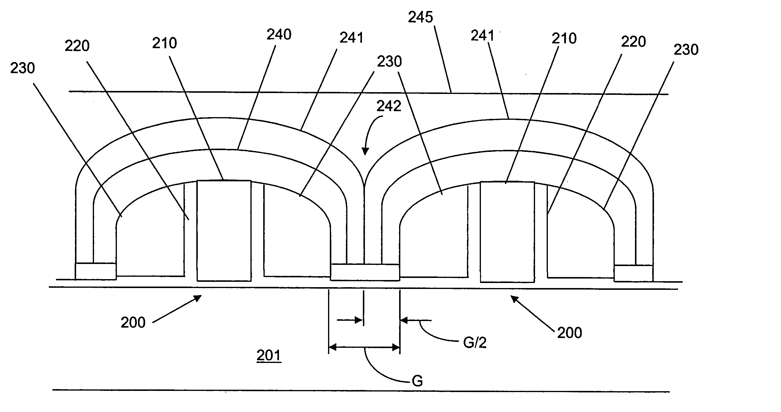
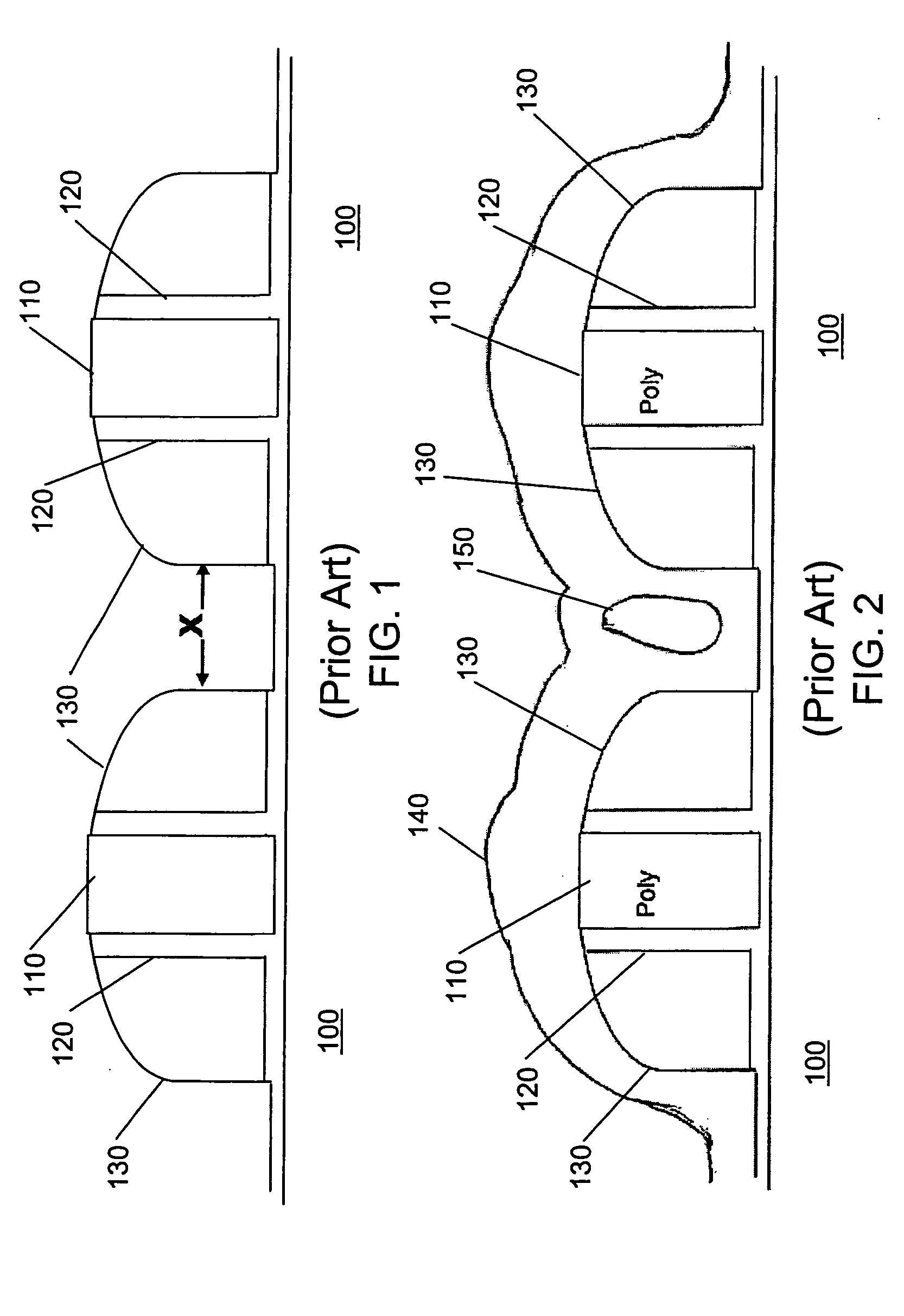
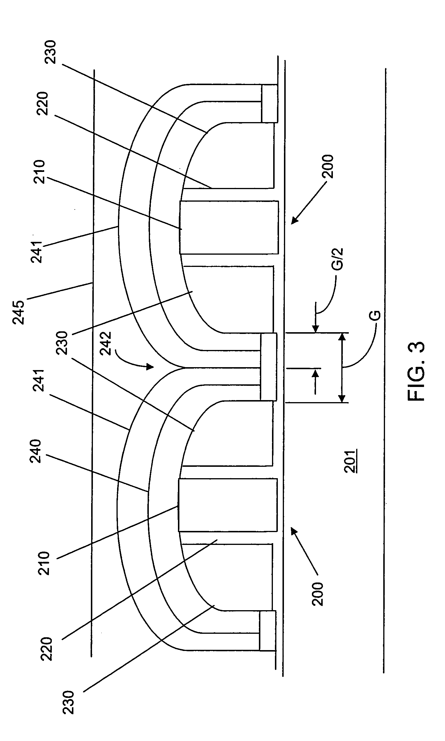
[0016] Methods and structures are described below, in which atomic layer deposition (ALD) is used to at least partially fill a gap or trench between devices. In some embodiments, ALD is used to form a liner for partially filling the gap or trench. In other embodiments, ALD is used to form an etch stop layer.

[0017] ALD uses sequen...


PUM


Abstract

A method is provided for filling a trench or gap between a pair of semiconductor devices formed above a substrate. A liner is applied in a trench or gap between a pair of devices by atomic layer deposition to partially fill the trench or gap. The trench or gap is filled by a bulk fill process.

Description

FIELD OF THE INVENTION [0001] The present invention relates to semiconductor fabrication generally, and more specifically to methods for filling gaps and trenches. BACKGROUND [0002] It is known in the prior art to provide isolation walls between adjacent devices or device regions in integrated circuits, such as CMOS integrated circuits. For example, these isolation walls have been formed of a dielectric such as phosphor silicate glass (PSG), silicon oxy-nitride, silicon dioxide, or a combination of silicon dioxide and polycrystalline silicon. [0003]FIG. 1 is a diagram of a pair of conventional devices 100, which may be thin film transistors, for example. Devices 100 may be any type of semiconductor device. In the example of FIG. 1, each device 100 has a polycrystalline silicon gate 110, gate dielectric 120 such as silicon nitride (SiN), and spacers 130, such as silicon oxy-nitride (SiOxNx) or TEOS. In this example, the devices are separated by a gap X. For many types of devices, suc...

Claims


Application Information

Patent Timeline
Patent Type & Authority Applications(United States)
IPC IPC(8): H01L21/314H01L21/316H01L21/76H01L21/768H01L21/8238
CPCH01L21/02129H01L21/02274H01L21/0228H01L21/823878H01L21/31625H01L21/76832H01L21/76837H01L21/3141
Inventor CHOU, YOU-HUALIOU, JOUNG-WEIHSU, KUANG-YUANLIN, CHIH-LUNGTSAI, CHENG-YUAN
Owner TAIWAN SEMICON MFG CO LTD
Why Eureka
Try Eureka