

Oxygen plasma treatment for enhanced HDP-CVD gapfill
- Summary
- Abstract
- Description
- Claims
- Application Information
AI Technical Summary
Benefits of technology
Problems solved by technology
Method used
Image

Examples
Embodiment Construction
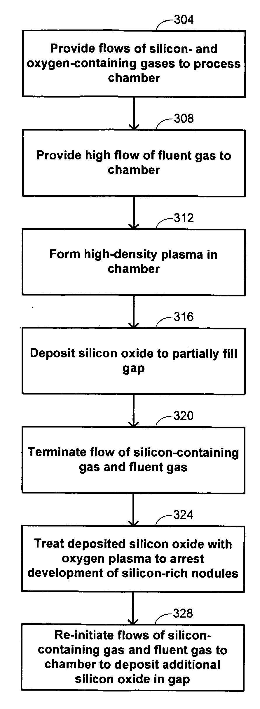
[0022] Embodiments of the invention are directed towards methods of depositing a silicon oxide film to fill a gap in a surface of a substrate using an HDP-CVD process. Silicon oxide films deposited according to the techniques described herein have excellent gapfill capabilities and are able to fill high-aspect-ratio gaps encountered in, for example, shallow-trench-isolation structures. In addition, the methods described herein result in films having good composition uniformity. Films deposited by the methods of the invention are thus suitable for use in the fabrication of a variety of integrated circuits, and are particularly useful in the fabrication of integrated circuits having minimum feature sizes of 0.13 microns or less.
[0023] As used herein, references to an HDP-CVD process are intended to refer to a plasma CVD process that includes simultaneous deposition and sputtering components, and that employs a plasma having an ion density on the order of 1011 ions / cm3 or greater. The...
PUM
| Property | Measurement | Unit |
|---|---|---|
| Fraction | aaaaa | aaaaa |
| Fraction | aaaaa | aaaaa |
| Time | aaaaa | aaaaa |
Abstract
Description
Claims
Application Information