Method for manufacturing printed circuit board and printed circuit board with gas venting hole

a technology of printed circuit board and venting hole, which is applied in the direction of manufacturing tools, soldering apparatus, non-printed masks, etc., can solve problems such as solder defects, and achieve the effect of more effective gas discharge performan

Inactive Publication Date: 2005-12-29
ORION ELECTRIC CO LTD
View PDF2 Cites 12 Cited by
  • Summary
  • Abstract
  • Description
  • Claims
  • Application Information

AI Technical Summary

Benefits of technology

[0022] According to the sixth aspect of the present invention related to the printed circuit board with a gas venting hole, wherein the diameter of the gas venting hole is within the range of 1.0 mm through 2.0 mm, the board can exert a more effective gas discharge performance in the dip soldering process. “The diameter of the gas venting hole being 1.0 mm or higher and 2.0 mm or smaller” discloses a most preferable range of diameter size that exerts an effective gas discharge ability but prevents leak of molten solder.

Problems solved by technology

In dip soldering, a flux is applied to the surface of the printed circuit board to be subjected to soldering in order to facilitate the soldering process, but when the flux is volatilized by the heat of the pre-heater and the molten solder, gas is generated which may cause solder defects.

Method used


Image

  • Method for manufacturing printed circuit board and printed circuit board with gas venting hole
  • Method for manufacturing printed circuit board and printed circuit board with gas venting hole
  • Method for manufacturing printed circuit board and printed circuit board with gas venting hole

Examples


embodiment 1

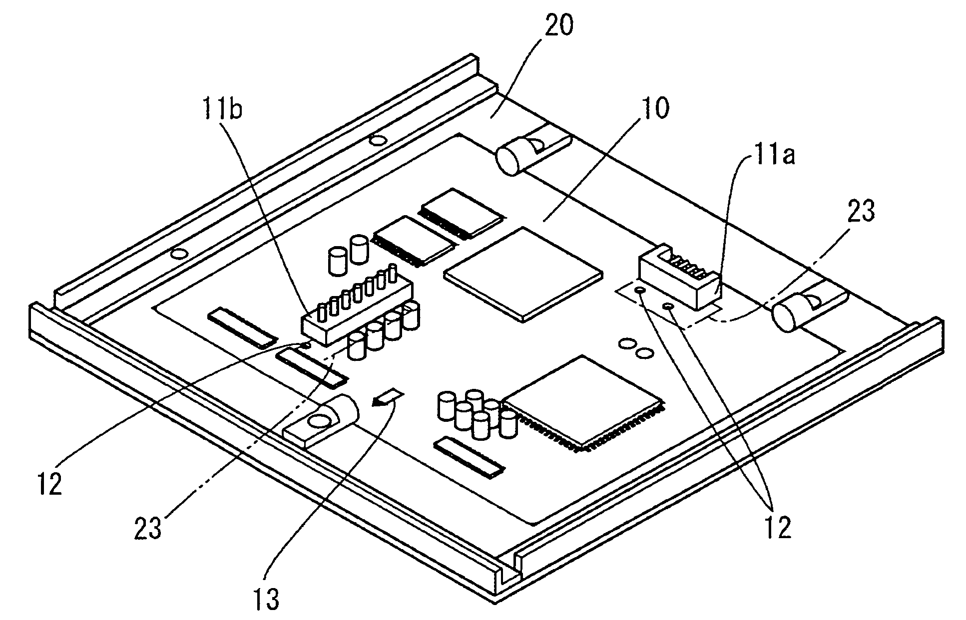
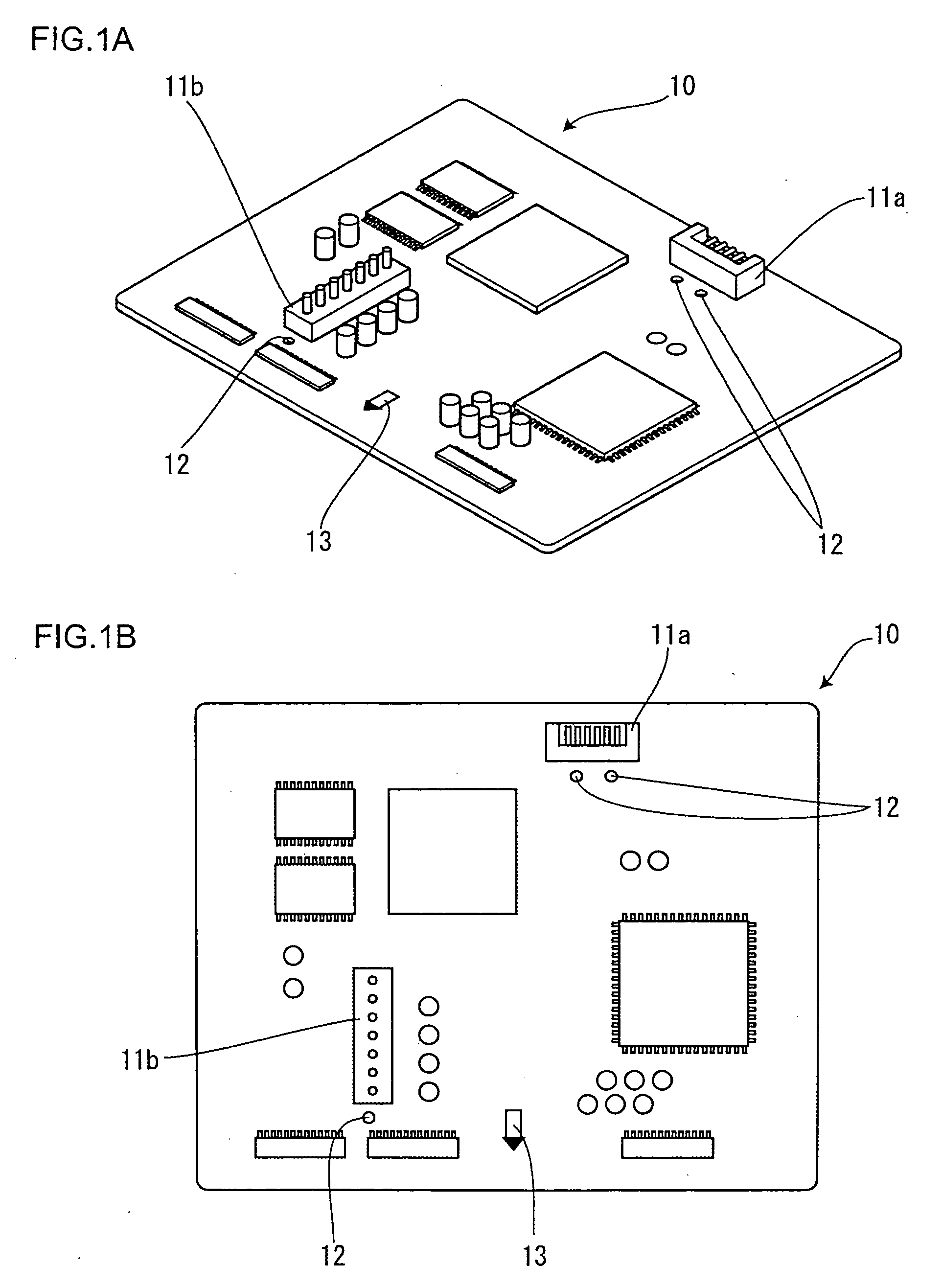
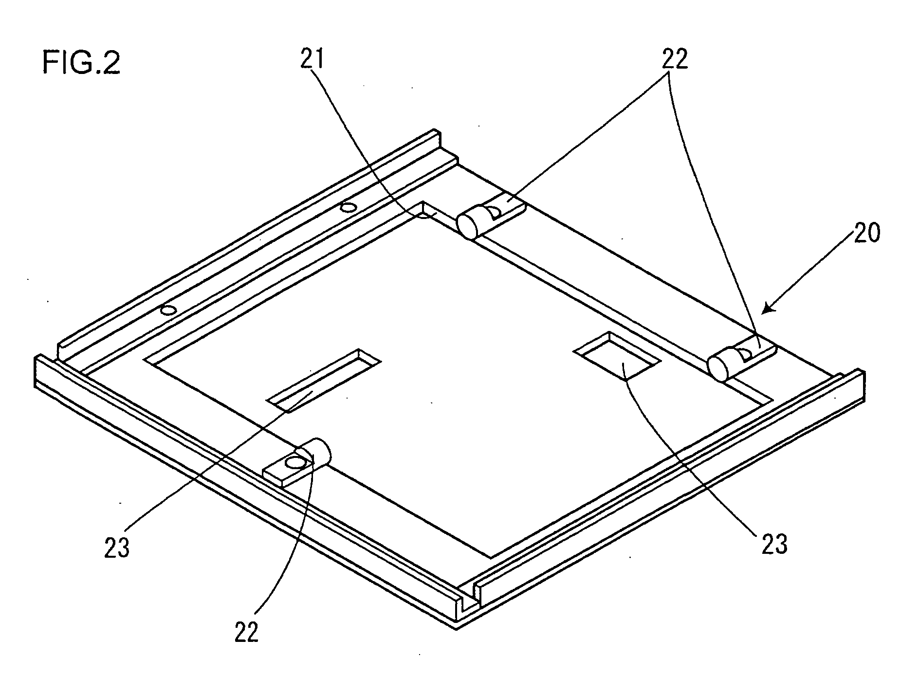
[0030]FIG. 1 is a perspective view showing the printed circuit board with a gas venting hole according to the present embodiment, wherein 1A is a perspective view and 1B is an upper view. FIG. 2 is a perspective view showing the dip soldering jig used in a dip soldering process. FIG. 3 is a schematic view showing the state in which the printed circuit board with a gas venting hole is attached to the dip soldering jig, wherein 3A is a perspective view and 3B is a cross-sectional concept view.

[0031] As illustrated in FIG. 1, a printed circuit board 10 includes electronic components (hereinafter called lead wire welding components) 11a and 11b wherein the electric connection to conductive patterns are performed via dip soldering, and has an arrow 13 showing the board feeding direction in the dip soldering process which is printed via serigraph. A dip soldering jig 20 comprises, as shown in FIG. 2, a recess 21, a stopper 22 and the like for positioning and stopping the printed circuit ...

embodiment 2

[0035]FIG. 6 is a flowchart showing the outline of the portion corresponding to the invention related to the method for manufacturing the printed circuit board of the present embodiment. The dip soldering jig used in the dip soldering process according to the present embodiment is the same as that of embodiment 1, and the printed circuit board being manufactured by the present embodiment is the same as that of embodiment 1. The same components are denoted with the same reference numbers, and detailed descriptions thereof are omitted.

[0036] The outline related to the present embodiment in the method of manufacturing the printed circuit board 10 will be described with reference to FIG. 6. The forming of gas venting holes 12 is simultaneously performed during a process for forming through holes etc. for mounting electronic components and through holes for engaging screws for fixing the substrate (step 61). As shown in FIGS. 1 and 4, the gas venting holes 12 are formed in areas adjacen...


PUM

PropertyMeasurementUnit
diameteraaaaaaaaaa
diameteraaaaaaaaaa
diameteraaaaaaaaaa

Abstract

The invention provides a printed circuit board to be subjected to dip soldering process using a dip soldering jig, the board capable of discharging gases generated by the volatilization of flux thereby preventing solder defects, and a method for manufacturing the printed circuit board. Gas venting holes 12 are formed in areas adjacent to lead wire welding components 11 on the forward side of the feeding direction of the printed circuit board in the dip soldering process (board feeding direction 13) and within the area of an opening 23 formed to the dip soldering jig 20. Thereby, gases generated during the dip soldering process are discharged efficiently.

Description

[0001] The present application is based on and claims priority of Japanese patent application No. 2004-185416 filed on Jun. 23, 2004, the entire contents of which are hereby incorporated by reference. BACKGROUND OF THE INVENTION [0002] 1. Field of the Invention [0003] The present invention relates to a printed circuit board on which electronic components are mounted, and especially, to a printed circuit board having electronic components soldered thereto via dip soldering, and the method for manufacturing the same. [0004] 2. Description of the Related Art [0005] A printed circuit board is formed by applying a conductive pattern formed by beaten copper onto an insulating plate, and electrically connecting various electric / electronic components to the conductive pattern. Usually, the electric connection between the conductive pattern and the electric / electronic components is realized via soldering, and one example of such soldering method is dip soldering. [0006] In dip soldering, a f...

Claims


Application Information

Patent Timeline
Patent Type & Authority Applications(United States)
IPC IPC(8): B23K1/00B23K31/00H05K3/34
CPCB23K1/0016B23K2201/42H05K3/3447H05K2203/1178H05K3/3468H05K2201/09063H05K2203/0557H05K3/3452B23K2101/42
Inventor SHIMADA, CHIKARATORII, SATOSHI
Owner ORION ELECTRIC CO LTD
Why Eureka
Try Eureka