Electric field reducing thrust plate

a technology of thrust plate and electric field, which is applied in the direction of manufacturing tools, electrical-based machining electrodes, machining electrodes, etc., can solve the problems of reducing the throughput of substrates, requiring additional process steps, and presenting several challenges to conventional plating methods and apparatuses. , to achieve the effect of reducing fluid flow

Inactive Publication Date: 2005-12-29
APPLIED MATERIALS INC
View PDF99 Cites 25 Cited by
  • Summary
  • Abstract
  • Description
  • Claims
  • Application Information

AI Technical Summary

Benefits of technology

[0008] The present invention generally provides a contact ring assembly for supporting a substrate in an electrochemical plating system comprising an annular contact ring having a plurality of substrate supporting electrical contact pins extending therefrom to provide electrical current to the surface of the substrate; a thrust

Problems solved by technology

However, electrochemical metallization of these features presents several challenges to conventional plating methods and apparatuses.
For example, one challenge associated with conventional plating apparatuses and methods is deposition on the bevel or backside of the substrate.
Although deposition on the bevel or backside of the substrate generally does not have a negative impact on the production surface of the substrate, the bevel or backside deposition must be removed, requiring additio

Method used


Image

  • Electric field reducing thrust plate
  • Electric field reducing thrust plate
  • Electric field reducing thrust plate

Examples


Embodiment Construction

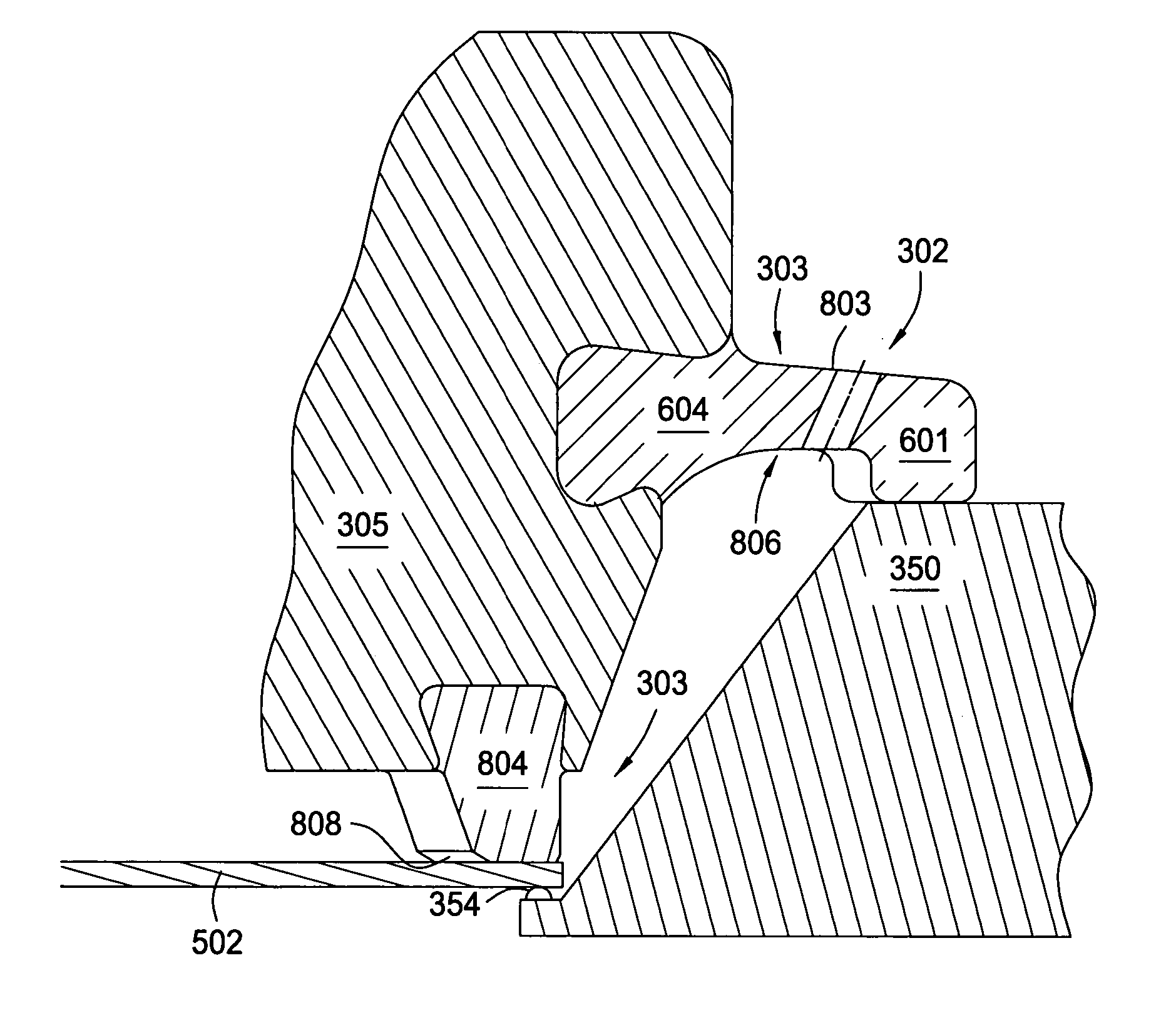
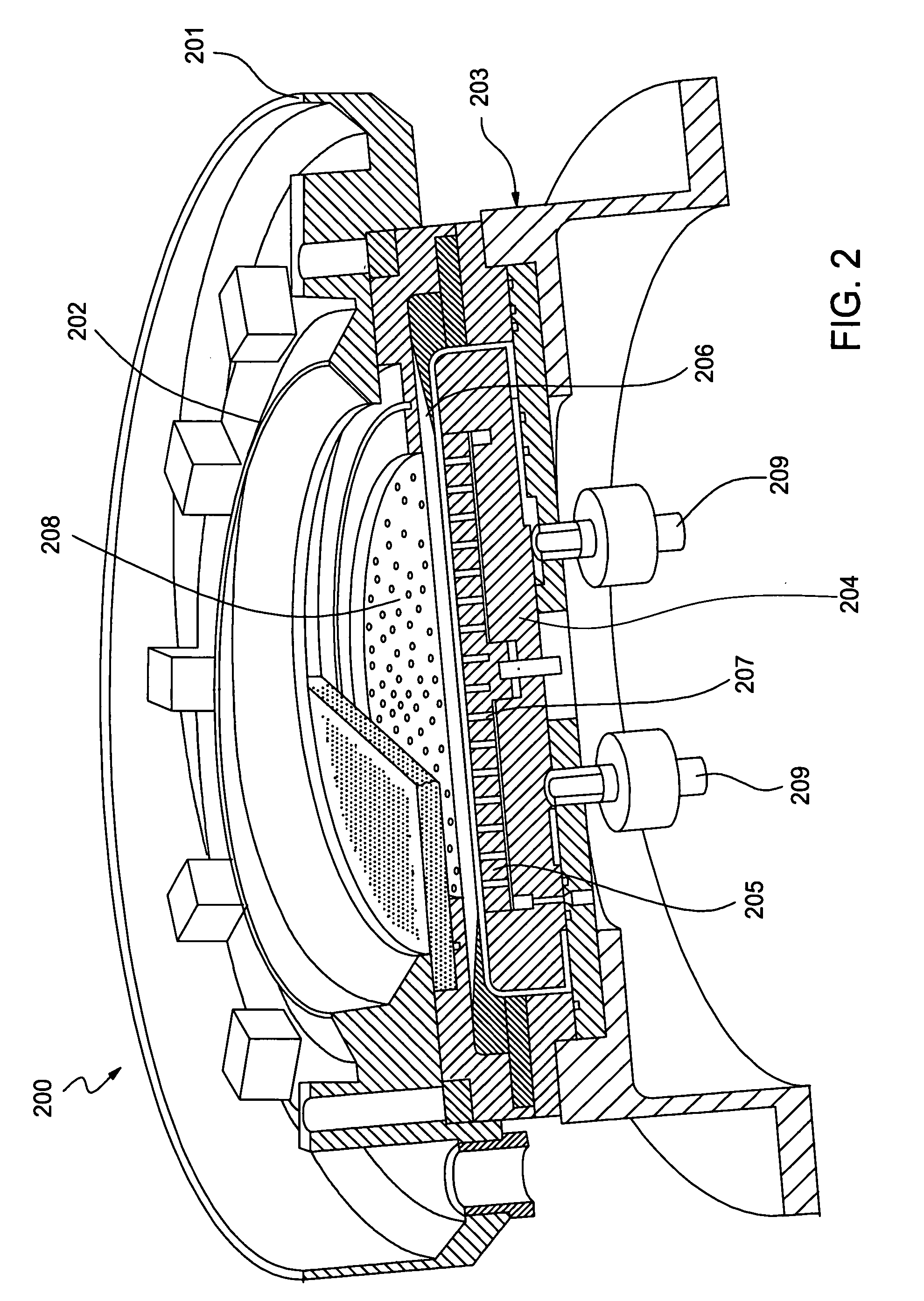
[0022] The present invention provides an electrolytic cell for semiconductor processing that includes an apparatus configured to minimize the electrical field proximate the bevel or backside of the substrate. Additionally, the invention provides a mechanism for the release of gas bubbles that may collect along the perimeter of the substrate and the contact ring.

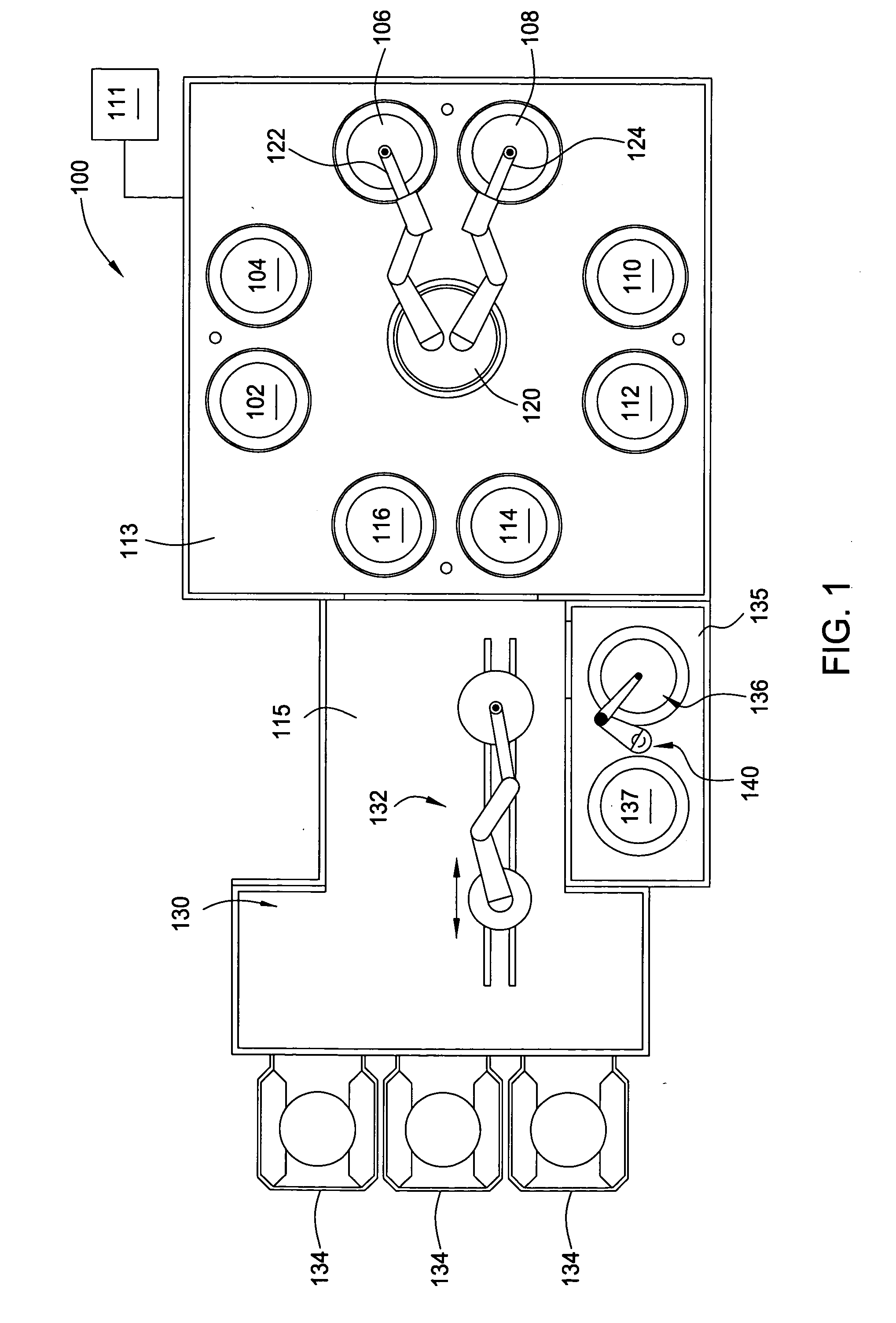
[0023]FIG. 1 is a top plan view of an exemplary electrochemical plating (ECP) system 100 that may be used to implement embodiments of the invention. ECP system 100 includes a factory interface 130, which is also generally described as a substrate loading location. Factory interface 130 includes a plurality of substrate loading locations configured to interface with substrate containing cassettes 134. A robot 132 is positioned in factory interface 130 and may access substrates (not shown) contained in the cassettes 134. Robot 132 also extends into a link tunnel 115 that connects factory interface 130 to processing mainframe 1...


PUM

PropertyMeasurementUnit
Flexibilityaaaaaaaaaa
Electric fieldaaaaaaaaaa

Abstract

A method and apparatus for an electrochemical processing cell that is configured to minimize bevel and backside deposition. The apparatus includes a contact ring assembly for supporting a substrate, a thrust plate movably positioned to engage a substrate positioned on the contact pins, and a lip seal member positioned to contact the thrust plate and the contact ring to prevent fluid flow therebetween. The lip seal includes a at least one bubble release channel formed therethrough. The method includes positioning an electric field barrier between a backside substrate engaging member and a frontside substrate supporting member to prevent electric field from traveling to the bevel and backside of the substrate. The electric field barrier including at least one bubble release channel formed therethrough.

Description

BACKGROUND OF THE INVENTION [0001] 1. Field of the Invention [0002] Embodiments of the invention are generally related to an apparatus and method for minimizing deposition on the bevel and backside of a substrate in an electrochemical deposition cell. [0003] 2. Description of the Related Art [0004] Metallization of high aspect ratio 90 nm and smaller sized features is a foundational technology for future generations of integrated circuit manufacturing processes. Metallization of these features is generally accomplished via an electrochemical plating process. However, electrochemical metallization of these features presents several challenges to conventional plating methods and apparatuses. For example, one challenge associated with conventional plating apparatuses and methods is deposition on the bevel or backside of the substrate. Although deposition on the bevel or backside of the substrate generally does not have a negative impact on the production surface of the substrate, the b...

Claims


Application Information

Patent Timeline
IPC IPC(8): C25D7/12C25D17/06H01L21/288
CPCC25D7/12H01L21/2885C25D17/06
Inventor HERCHEN, HARALDLUBOMIRSKY, DMITRYZHENG, BOPANG, LILY L.
Owner APPLIED MATERIALS INC
Why Eureka
Try Eureka