Method and apparatus for measuring three-dimensional shape of specimen by using SEM

a three-dimensional shape and specimen technology, applied in the field of methods and apparatus for measuring or estimating the three-dimensional profile of specimens, can solve the problems of difficult to accurately estimate the height information on a flat portion or a nearly vertical portion, and the pre-process for manufacturing these devices is becoming increasingly difficult to control, so as to achieve accurate measurement of the three-dimensional profile

Active Publication Date: 2005-12-29
HITACHI HIGH-TECH CORP
View PDF9 Cites 33 Cited by
  • Summary
  • Abstract
  • Description
  • Claims
  • Application Information

AI Technical Summary

Benefits of technology

[0006] The present invention has been devised to solve the above problems. It is, therefore, an object of the present invention to provide a method and apparatus for measuring a three-dimensional profile using an SEM,

Problems solved by technology

With the miniaturization of semiconductor devices, the pre-process for manufacturing these devices is becoming increasingly difficult to control.
However, since the sensitivity to the inclination an

Method used


Image

  • Method and apparatus for measuring three-dimensional shape of specimen by using SEM
  • Method and apparatus for measuring three-dimensional shape of specimen by using SEM
  • Method and apparatus for measuring three-dimensional shape of specimen by using SEM

Examples


Embodiment Construction

[0030] There will now be described methods and apparatuses for measuring a three-dimensional profile using an SEM (Scanning Electron Microscope) according to preferred embodiments of the present invention with reference to the accompanying drawings.

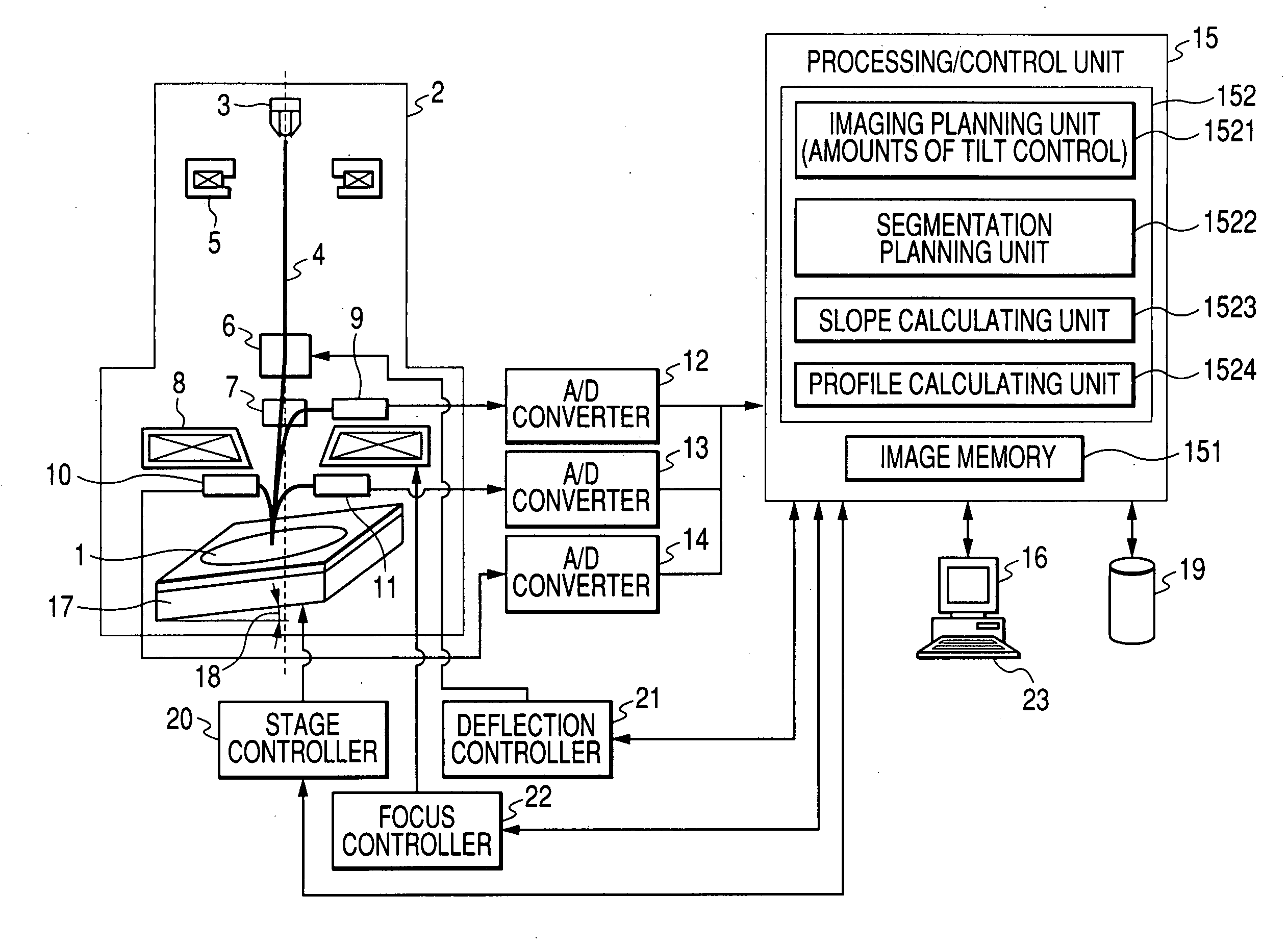
[0031]FIG. 1 is a diagram showing a system for obtaining and processing an SEM image according to an embodiment of the present invention. As shown in the figure, an electron optical system 2 comprises an electron beam source (an electron gun) 3 for emitting an electron beam 4, a condensing lens 5, a deflector 6, an ExB deflector 7, an objective lens 8, a secondary electron detector 9, and reflected electron detectors 10 and 11. Reference numeral 17 denotes a stage (X-Y-Z stage) on which a specimen 1 (e.g., a semiconductor wafer) is placed. The stage 17 includes a tilt stage for forming a stage tilt angle 18. It should be noted that the stage 17 can be tilted in the X- and Y-directions about tilt axes as a center which is substantially a ...


PUM


Abstract

The present invention relates to a method and apparatus for measuring a three-dimensional profile using a SEM, capable of accurately measuring the three-dimensional profile of even a flat surface or a nearly vertical surface based on the inclination angle dependence of the amount of secondary electron image signal detected by the SEM. Specifically, a tilt image obtaining unit obtains a tilt image (a tilt secondary electron image) I(2) of flat regions a and c1 on a pattern to be measured by using an electron beam incident on the pattern from an observation direction φ(2). Then, profile measuring units presume the slope (or surface inclination angle) at each point on the pattern based on the obtained tilt image and integrate successively each presumed slope value (or surface inclination angle value) to measure three-dimensional profiles S2a and S2c. This arrangement allows a three-dimensional profile to be accurately measured.

Description

BACKGROUND OF THE INVENTION [0001] The present invention relates to a method and apparatus for measuring or estimating the three-dimensional profile of a specimen such as a semiconductor wafer in a semiconductor manufacturing process based on images obtained by observing the specimen using an SEM (Scanning Electron Microscope) when the specimen is observed or measured. [0002] With the miniaturization of semiconductor devices, the pre-process for manufacturing these devices is becoming increasingly difficult to control. The electrical characteristics of a semiconductor device pattern are very much affected by its height and line width and the inclination angles of the sidewalls, as well as minute pattern shape variations such as the roundness of the corners. As such, there has been a need to accurately measure these dimensions and shapes to detect process variations and thereby control the process. Thus, effectively controlling the manufacturing process of a semiconductor device requ...

Claims


Application Information

Patent Timeline
IPC IPC(8): H01J37/28
CPCH01J2237/2814H01J37/28
Inventor TANAKA, MAKIMIYAMOTO, ATSUSHIMOROKUMA, HIDETOSHISHISHIDO, CHIEIKEDA, MITSUJITOYODA, YASUTAKA
Owner HITACHI HIGH-TECH CORP
Why Eureka
Try Eureka