Organic electroluminescent display device and method of preparing the same

a technology of electroluminescent display device and electroluminescent screen, which is applied in the direction of luminescent screen, discharge tube, identification means, etc., can solve the problems of poor light extraction efficiency, achieve superior image quality, improve light extraction efficiency, and improve light extraction efficiency

Active Publication Date: 2005-12-29
SAMSUNG DISPLAY CO LTD
View PDF9 Cites 20 Cited by
  • Summary
  • Abstract
  • Description
  • Claims
  • Application Information

AI Technical Summary

Benefits of technology

[0008] The present invention provides an organic electroluminescent display (OLED) device that may have superior light extraction efficiency and resistance to moisture and oxygen infiltration, and a method of fabricating the same. The OLED device may include a substrate on which a first electrode is provided. A second electrode is formed so as to be insulated from the first electrode. One or more organic layers may be interposed between the first electrode and the second electrode and may include at least an emission layer. One layer or a plurality of layers may be formed on the second electrode and may comprise a material or materials having a refractive index that is higher than a refractive index of a material forming the second electrode.
[0009] The organic electroluminescent display device of the present invention as described above may exhibit superior image quality due to both improved efficiency of light extraction and color purity. Also, the organic electroluminescent display device of the present invention has an improved lifespan due to its protection from moisture and oxygen infiltration of an emission part comprising a first electrode, a second electrode, and an organic layer.

Problems solved by technology

Nevertheless, the lifespan of the OLED taught by Korean Patent Publication No. 2001-0067868 may not reach satisfactory levels and may have poor light extraction efficiency, and thus improvement is needed.

Method used


Image

  • Organic electroluminescent display device and method of preparing the same
  • Organic electroluminescent display device and method of preparing the same
  • Organic electroluminescent display device and method of preparing the same

Examples


example 1

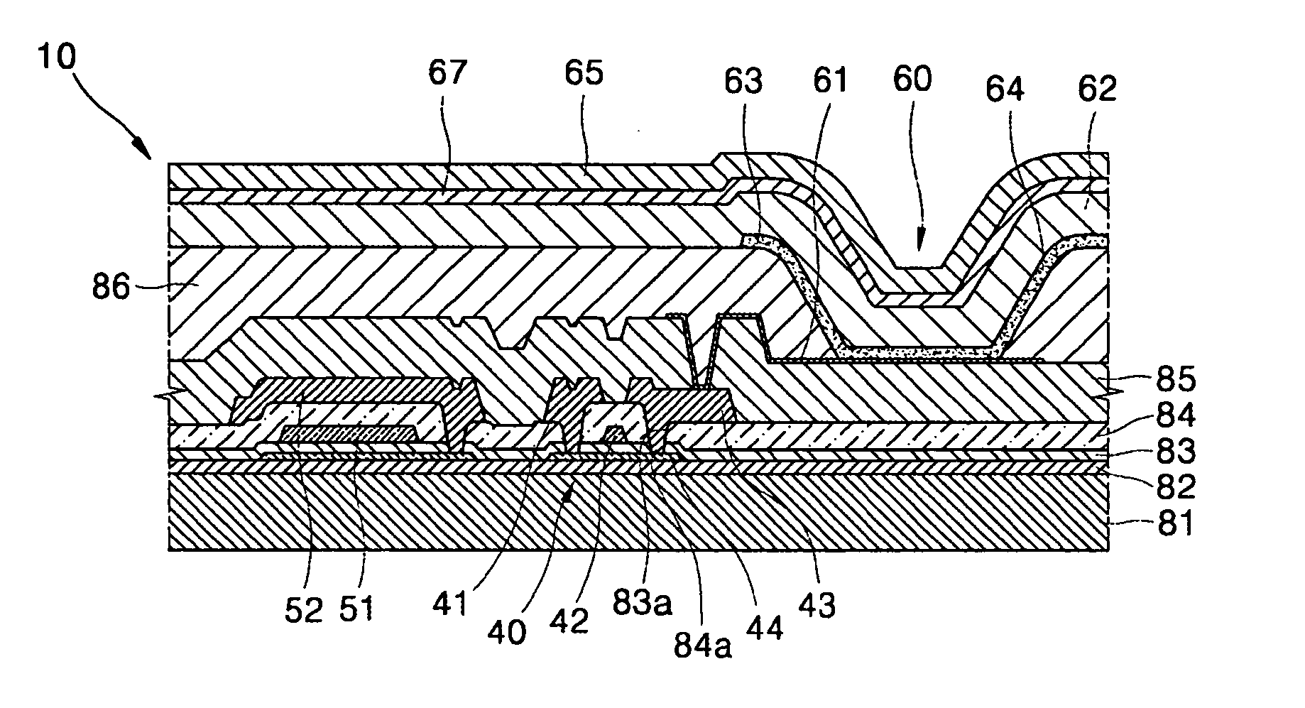
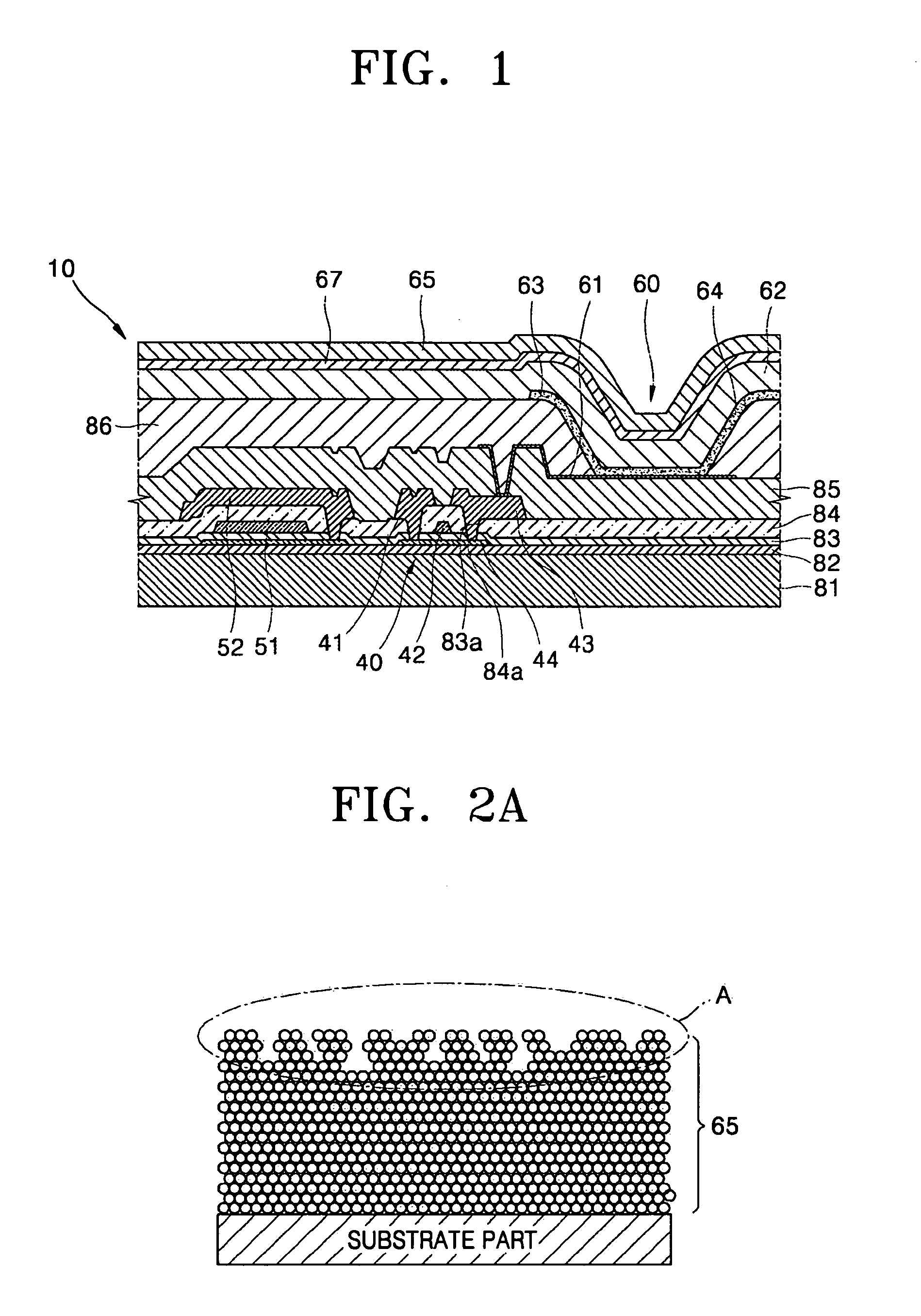
[0053] ITO, PEDOT with a thickness of 500 Å, PPV with a thickness of 800 Å, LiF with a thickness of 10 Å, and Mg:Ag with a thickness of 160 Å were sequentially laminated on a glass substrate and a SnOx layer with a thickness of 400 Å was formed on the Ag layer using a thermal deposition method. Thereafter, 1 g of silicon oxide powder was prepared as a silicon oxide deposition source and 1 g of Sn was prepared as a Sn deposition source. Then, a container including the silicon oxide deposition source, the Sn deposition source, an ion beam source, a thermal evaporation source, a substrate holder, and a rotation shaft for rotating the substrate holder was prepared. Those prepared as described above were used as the silicon oxide deposition source and the Sn deposition source, an EndHall-type ion gun (available from Infovion Co., Ltd.) was used as the ion beam source, and Helisys (available from ANS Co., Ltd.) was used as the thermal evaporation source. The prepared substrate was mounted...

example 2

[0055] Sample 2 was prepared in the same manner as in Example 1, except that a SiSnO layer with a thickness of 300 Å rather than 800 Å was formed.


PUM


Abstract

The present invention provides an organic electroluminescent display device and a method of preparing the same. The organic electroluminescent display device may include a first electrode formed on a substrate. A second electrode may be formed so as to be insulated from the first electrode. One or more organic layers may be interposed between the first electrode and the second electrode and include at least an emission layer. One layer or a plurality of layers may be formed on the second electrode and comprise a material or materials having a refractive index higher than a refractive index used to form a material that comprise the second electrode. An organic electroluminescent display device fabricated in this matter has improved efficiency of light extraction. Such a device also resists infiltration of moisture and oxygen to a luminous part of the device that includes the first electrode, the second electrode, and the organic layer.

Description

CROSS-REFERENCE TO RELATED APPLICATIONS [0001] This application claims priority to Korean Patent Application No.10-2004-0042211, filed on Jun. 9, 2004 and to Korean Patent Application No.10-2004-0045031, filed on Jun. 17, 2004, in the Korean Intellectual Property Office, the disclosures of which are herein incorporated by reference in their entireties. BACKGROUND OF THE INVENTION [0002] 1. Field of the Invention [0003] The present invention generally relates to flat panel display devices and methods for fabricating the same and, more particularly, to an organic electroluminescent display (OLED) device that may have superior efficiency of light extraction and superior resistance to moisture and oxygen infiltration, and to a method of manufacturing the same. [0004] 2. Description of Related Art [0005] Flat panel displays may be categorized as emissive devices or as non-emissive devices. Examples of emissive devices are a flat cathode ray tube (CRT), a plasma display panel, an electrol...

Claims


Application Information

Patent Timeline
Patent Type & Authority Applications(United States)
IPC IPC(8): G09F9/30H01J1/62H05B33/02H01J63/04H01L27/32H01L51/50H01L51/52H05B33/10H05B33/14H05B33/22H05B33/26
CPCH01L51/5262H01L51/5237H10K50/85H10K50/844
Inventor HAN, DONG-WONLEE, KWAN-HEEKWON, JANG-HYUK
Owner SAMSUNG DISPLAY CO LTD
Why Eureka
Try Eureka