Stacked transistor method and apparatus

a transistor and stacking technology, applied in the field of integrated electronic circuits, can solve the problems of undesired signal energy not only consuming circuit power, but also requiring filtering, and the type output of such amplifiers generally requires extensive filtering

Active Publication Date: 2005-12-29
PSEMI CORP
View PDF19 Cites 66 Cited by
  • Summary
  • Abstract
  • Description
  • Claims
  • Application Information

AI Technical Summary

Problems solved by technology

The PA subcircuit is typically the most power-consuming portion of such transmitters, and, also typically, is the source of the most significant unintended or “spurious” emissions.
However, the pulse-type outputs from such amplifiers generally require extensive filtering in order to establish a narrow-band sinusoidal output, as is typically required.
While normal operation of class D-F PAs does not intentionally cause drive element devices to conduct while voltage is present across the devices, even switched devices consume real power due to current flowing while voltage is present during finite switching periods.
The higher frequency signals include significant energy at undesired frequencies, and such undesired signal energies not only consume circuit power, but also require filtering to meet emission limits.
However, integrated circuit (IC) FETs have a limited capability to withstand voltage between any two nodes, including gate-source, gate-drain, and drain-source node pairs.
Such voltage withstand limitations may particularly impair the usefulness of IC FETs in high power switching circuits, in which inductive voltages may greatly exceed the supply voltage.
One of the difficulties with existing PA technologies is that many otherwise desirably high-speed devices are fabricated using processes that tend to yield FETs having relatively low breakdown voltages.

Method used


Image

  • Stacked transistor method and apparatus
  • Stacked transistor method and apparatus
  • Stacked transistor method and apparatus

Examples


Embodiment Construction

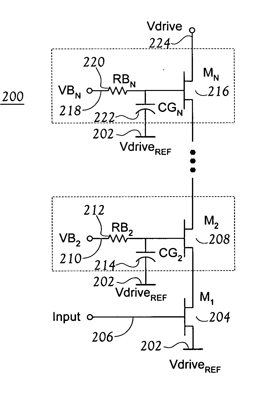
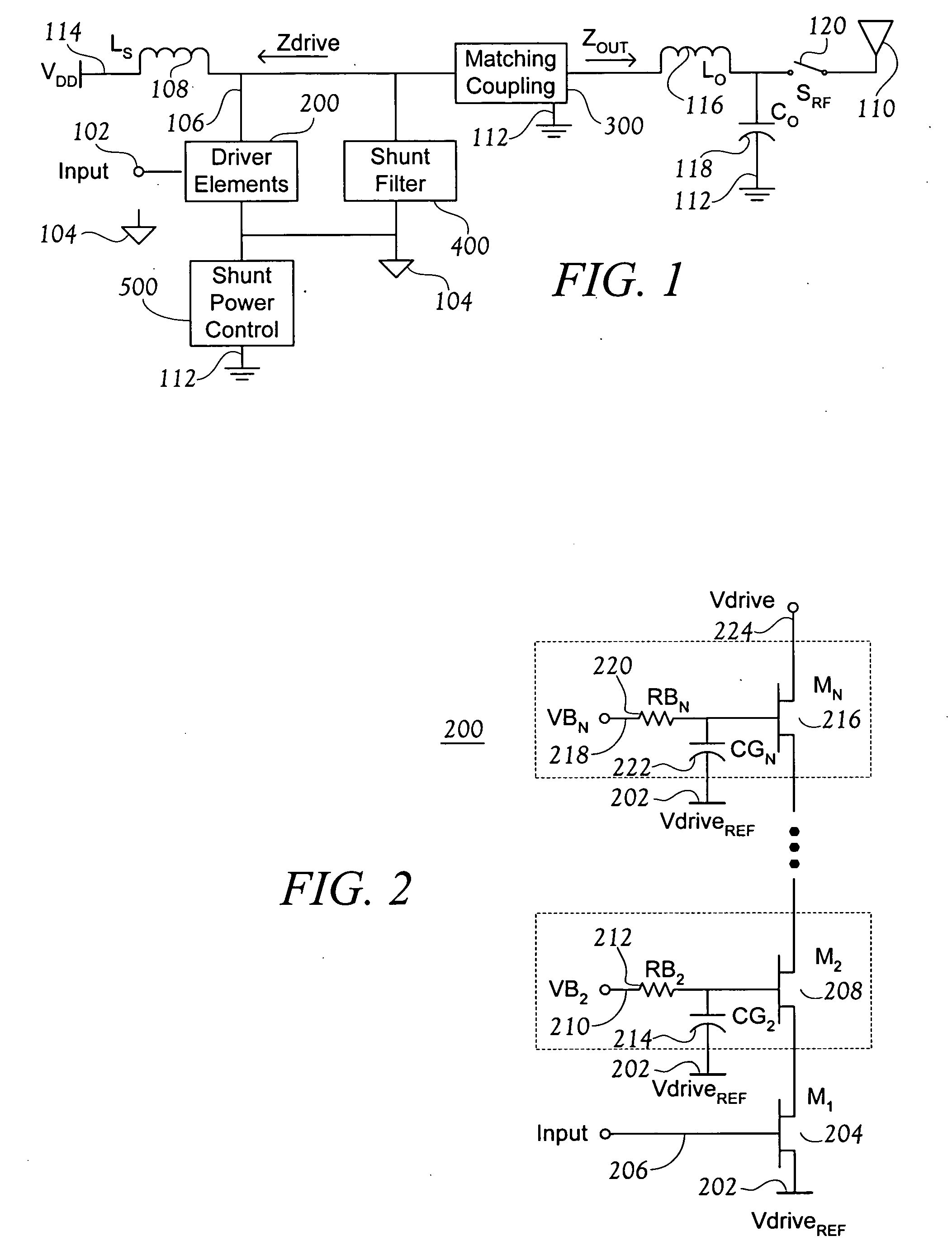
[0028] Power Amplifier Overview

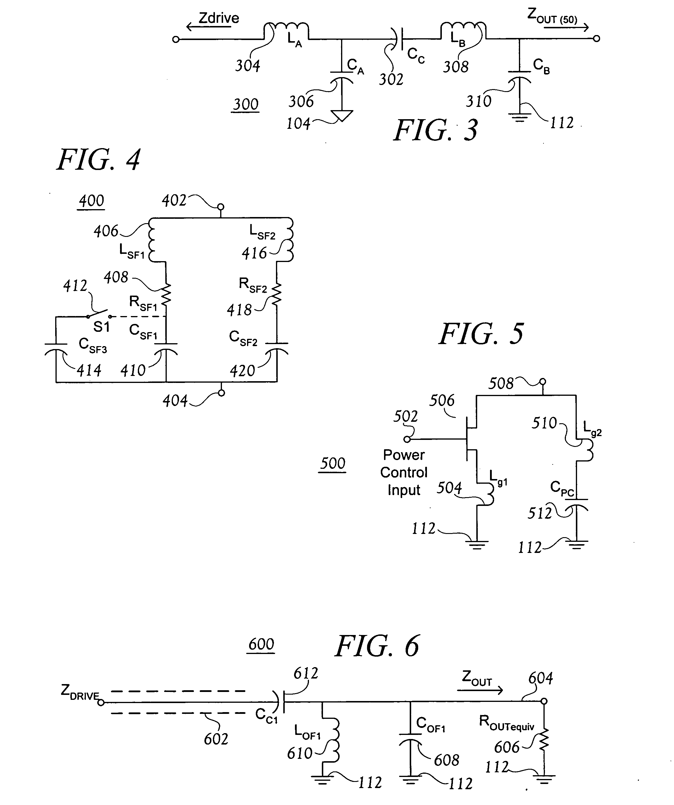
[0029]FIG. 1 is a block diagram of an RF power amplifier (PA). The illustrated RF PA is quite general, in that varying the biasing of devices in a driver elements block 200, and / or varying details of the other blocks, will permit the RF PA illustrated in FIG. 1 to operate in any of classes A, B, C, E or F. FIGS. 2-5 each show an exemplary circuit to implement one of the blocks shown in FIG. 1.

[0030] An input 102 is provided to the PA with respect to a circuit reference, or common, 104. The input 102 generally comprises a properly biased signal at a center drive frequency, f0. In response to the input 102, the driver elements block 200 controls conduction between a drive output node 106 and the circuit common 104. The driver elements block 200, in conjunction with current from VDD via an RF choke Ls 108, provides a signal having a particular impedance Zdrive. Zdrive may vary with frequency, but will refer to the drive impedance at the center operating...


PUM


Abstract

A method and apparatus is described for controlling conduction between two nodes of an integrated circuit via a stack of FETs of common polarity, coupled in series. In an RF Power Amplifier (PA) having appropriate output filtering, or in a quad mixer, stacks of two or more FETs may be used to permit the use of increased voltages between the two nodes. Power control for such RF PAs may be effected by varying a bias voltage to one or more FETs of the stack. Stacks of three or more FETs may be employed to control conduction between any two nodes of an integrated circuit.

Description

[0001] This application is related to co-pending and commonly assigned U.S. application Ser. No. 10 / 267,531, filed Oct. 8, 2002, entitled “Switch Circuit and Method of Switching Radio Frequency Signals,” which claims the benefit under 35 U.S.C. § 119 (e) of U.S. Provisional Application No. 60 / 328,353, filed Oct. 10, 2001, entitled “Silicon-on-Insulator RF Switches,” both of which applications are hereby incorporated in their entirety by reference.BACKGROUND OF THE INVENTION [0002] 1. Field of the Invention [0003] This invention relates broadly to integrated electronic circuits, and more specifically to FET circuits for controlling voltages that exceed individual FET breakdown voltages. [0004] 2. Related Art [0005] Wireless communications devices, especially handheld devices, are undergoing sustained development. Perhaps more than any other factor, the extreme popularity of cellular mobile telephones has motivated improvements in efficiency, speed, and cost-effectiveness for RF trans...

Claims


Application Information

Patent Timeline
Patent Type & Authority Applications(United States)
IPC IPC(8): H03F1/22H03F3/189H03F3/68H04B1/28H04M1/00
CPCH03F1/223H03F3/189H03F3/2171H03F2200/61H03F2200/294H03F2200/372H03F3/68H01Q23/00H03F1/565H03G3/3042H03G11/00H04B1/0475H04B1/48
Inventor BURGENER, MARK L.CABLE, JAMES S.
Owner PSEMI CORP
Why Eureka
Try Eureka