Eureka AIR delivers breakthrough ideas for toughest innovation challenges, trusted by R&D personnel around the world.

Circuit board electrode connection structure

Inactive Publication Date: 2005-12-29
SHARP KK
View PDF5 Cites 35 Cited by
  • Summary
  • Abstract
  • Description
  • Claims
  • Application Information

AI Technical Summary

Benefits of technology

[0020] In accordance with embodiment(s) of the present invention having such feature(s), adhesive(s) containing epoxy-type resin(s) (for which coefficient of linear expansion is 60 ppm / ° C. to 150 ppm / ° C.) and / or the like, which typically have coefficient(s) of linear expansion greater than that or those of board substrate(s) of the circuit board(s) (coefficient of linear expansion for glass epoxy is 10 ppm / ° C. to 50 ppm / ° C.; coefficient of linear expansion for polyimide is 12 ppm / ° C. to 20 ppm / ° C.), Cu or other such electrode metal material(s) (for which coefficient of linear expansion is 10 ppm / ° C. to 20 ppm / ° C.), or device substrate(s) (coefficient of linear expansion for piezoelectric material (PZT) is 2 ppm / ° C. to 6 ppm / ° C.; coefficient of linear expansion for semiconductor material is 3 ppm / ° C. to 5 ppm / ° C.) may be thinner than would be the case in a conventional electrode connection structure, even where the adhesive(s) is / are present in intervening fashion at the electrode connection region(s) so as to electrically and mechanically connect a plurality of the circuit boards. This being the case, thermal stresses during temperature rises acting in direction(s) tending to cause mutual separation of the electrodes, e.g., between the device substrate and the circuit board or between two of the circuit boards which are connected together, can be reduced, permitting prevention of occurrence of electrical continuity failures, since the relative contribution due to that or those material(s) other than the adhesive(s) which, among the various material(s) employed in forming the constituent members of the electrode connection region(s), has or have the largest coefficient(s) of linear expansion increases. Furthermore, because the magnitude of strain resulting from thermal stresses can be reduced, it is possible to prevent early deterioration in reliability with thermal cycling, making it possible to achieve a circuit board electrode connection structure having high reliability.
[0030] As described above, a circuit board electrode connection structure in accordance with embodiment(s) of the present invention may be such that the adhesive(s) is / are thinner than would be the case in a conventional electrode connection structure, even where the adhesive(s), which contain epoxy-type resin(s) and / or other such substance(s) typically having coefficient(s) of linear expansion greater than that or those of the constituent members of the electrode connection region(s)—i.e., board substrate(s) of the circuit board(s), the electrode metal material(s), and / or the device substrate(s)—is / are present in intervening fashion at the electrode connection region(s) so as to electrically and mechanically connect the circuit boards. This being the case, thermal stresses during temperature rises acting in direction(s) tending to cause mutual separation of the electrodes, e.g., between the device substrate and the circuit board or between two of the circuit boards which are connected together, can be reduced, as a result of which it is possible to prevent occurrence of electrical continuity failures, since the relative contribution due to that or those material(s) other than the adhesive(s) which, among the constituent members of the electrode connection region(s), has or have the largest coefficient(s) of linear expansion increases. Furthermore, because the magnitude of strain resulting from thermal stresses can be reduced, it is possible to prevent early deterioration in reliability with thermal cycling, making it possible to achieve a circuit board electrode connection structure having high reliability.

Problems solved by technology

A variety of problems such as the following can arise when a conventional circuit board connection structure as has been described above is employed to connect device(s) to circuit board(s) or is employed to connect circuit board(s) to circuit board(s).
, because a rise in temperature at the electrode connection region will cause adhesive at the electrode connection region to expand by a large amount, with thermal stresses acting in a direction such as will tend to spread the electrodes apart, there has been the problem of occurrence of electrical continuity failures. F
urthermore, there has been the problem that the high magnitude of the strain experienced by adhesive with change in temperature causes adhesive force to deteriorate, and there has been the problem of early failure during thermal cycling reliability testing.
Furthermore, just as was the case for the inkjet head electrode connection structure described above, conventional electrode connection structures between circuit boards, e.g., such as those between flexible wiring board(s) and rigid wiring board(s), have the problems of electrical continuity failures at elevated temperature and early deterioration in reliability with thermal cycling.

Method used


Image

  • Circuit board electrode connection structure
  • Circuit board electrode connection structure
  • Circuit board electrode connection structure

Examples


embodiment 1

[0045] Below, a first embodiment of the present invention is described with reference to the drawings.

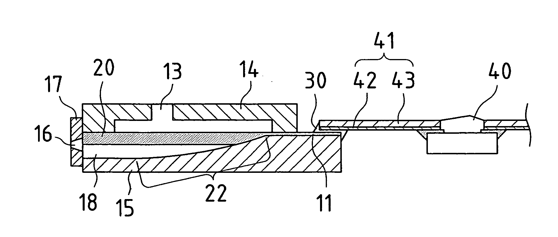
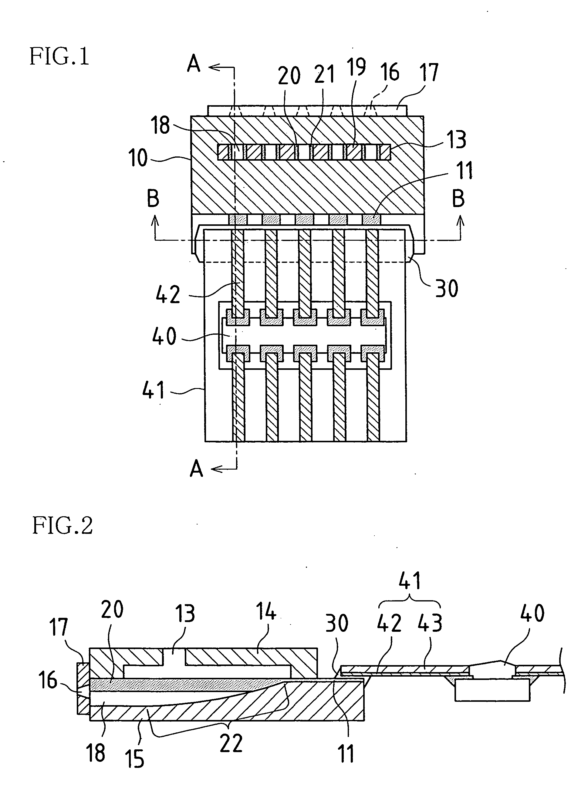
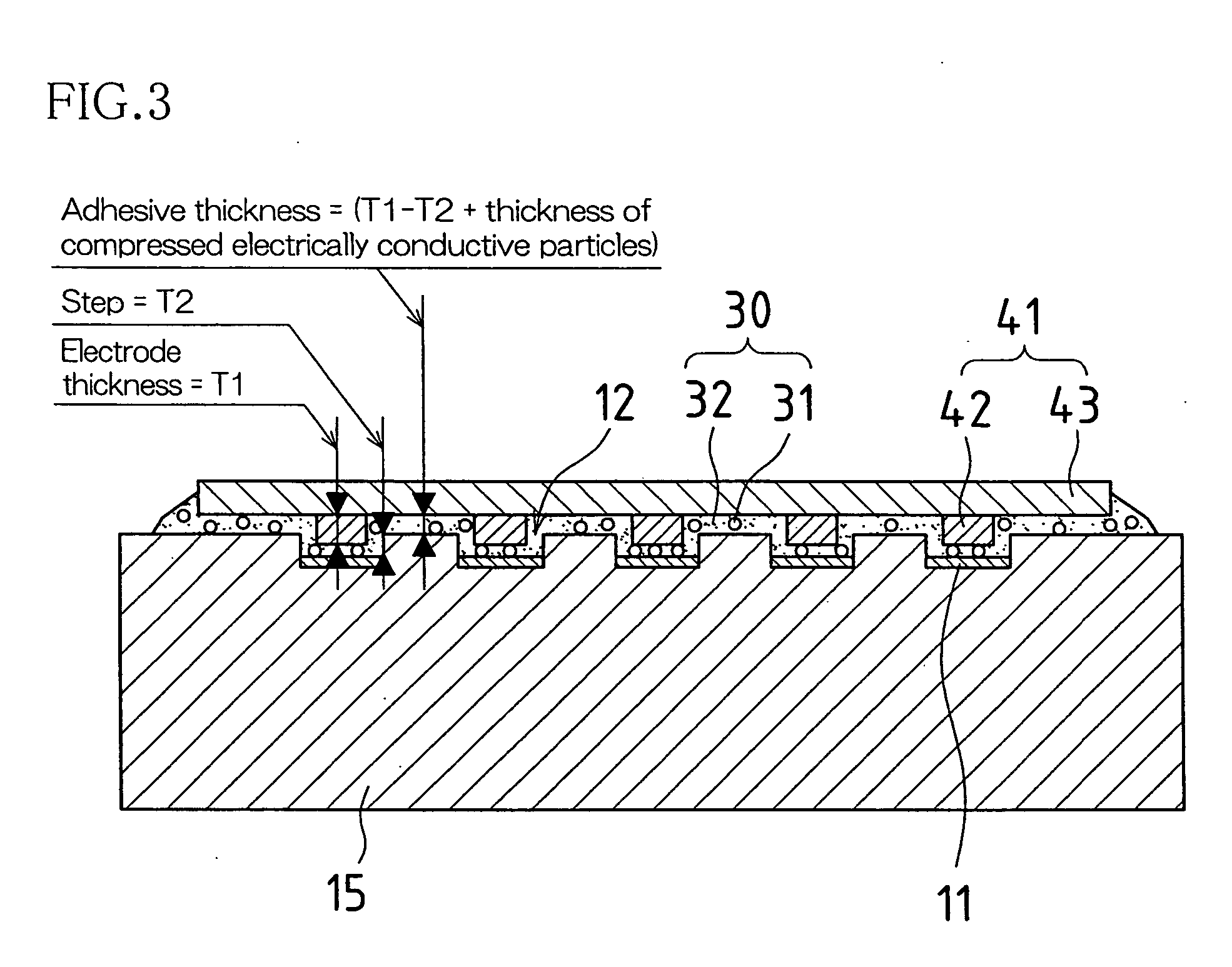
[0046]FIG. 1 is a sectional view showing a circuit board electrode connection structure associated with the first embodiment of the present invention as seen in plan view; FIG. 2 is a cross-sectional view of section A-A in FIG. 1; and FIG. 3 is a cross-sectional view of section B-B in FIG. 1.

[0047] In the present first embodiment, an inkjet head employing anisotropic electrically conductive adhesive is used as example of an object being bonded; and a flexible wiring board (here, a TCP; i.e., tape carrier package) is used as an example of a circuit board.

[0048] As shown in FIGS. 1 through 3, electrode connection structure(s) at inkjet head(s) 10 is / are such that outer lead(s) 42 is / are formed on TCP(s) 41 on which inkjet head drive IC(s) 40 is / are mounted; the structure being such that electrical and mechanical connection to external circuitry connection electrode(s) 11 of inkjet ...

embodiment 2

[0061] Next, a second embodiment of the circuit board electrode connection structure of the present invention is described with reference to the drawings.

[0062]FIG. 7 is a sectional view showing a circuit board electrode connection structure associated with the second embodiment of the present invention.

[0063] At the present second embodiment, a circuit board electrode connection structure in which adhesive is used to connect two circuit boards is described. A glass epoxy wiring board is used as one of the circuit boards, and a flexible wiring board is used as the other of the circuit boards.

[0064] Glass epoxy wiring board 70 is made up of glass epoxy substrate 71 and electrode(s) 72. Electrode 72 is such that Ni and Au plating is applied over ½ oz. copper foil wiring (thickness 18μ) formed over glass epoxy board substrate 71, this protruding from glass epoxy substrate 71 to a thickness (T5) of approximately 20μ.

[0065] On the other hand, flexible wiring board 80 is made up of po...


PUM


Abstract

An electrode connection structure between outer lead(s) of TCP(s), being first circuit board(s), and actuator member electrode(s) for connection to external circuitry, being second circuit board(s); actuator member(s) electrode(s) for connection to external circuitry being formed in or on floor(s) of recess(es) which is / are step(s) smaller in magnitude than thickness(es) of outer lead(s) protruding from polyimide substrate(s) of TCP(s); adhesive(s) having thickness(es) more or less equal to difference(s) between step(s) and thickness(es) of outer lead(s); and outer lead(s) being electrically and mechanically connected to electrode(s) for connection to external circuitry.

Description

BACKGROUND OF INVENTION [0001] This application claims priority under 35 USC 119(a) to Patent Application No. 2004-185351 filed in Japan on 23 Jun. 2004, the content of which is hereby incorporated herein by reference in its entirety. [0002] The present invention relates to an electrode connection structure for use between / among circuit boards and to an electrode connection structure for use between / among inkjet head(s), semiconductor device(s), liquid crystal display panel(s), MEMS (microelectromechanical system) device(s), and / or the like and circuit board(s) such as flexible wiring board(s). [0003] An electrode connection structure for use between an inkjet head and a flexible wiring board is proposed at Japanese Patent Application Publication Kokai No. 2002-127422 and elsewhere. [0004] Referring to FIG. 9 (a) through (b), a conventional inkjet head will be described in general terms. [0005] An ink chamber comprising a plurality of grooves is formed by lamination of actuator memb...

Claims


Application Information

Patent Timeline
IPC IPC(8): H05K1/14H01R12/51H05K3/32H05K3/36
CPCB41J2/14209B41J2/1609B41J2/1623B41J2/1631B41J2/1632B41J2/1635H05K2201/09472B41J2/1643B41J2002/14491H05K3/323H05K3/361H05K2201/0352B41J2/1642
Inventor SAKAMOTO, YASUHIROSAGARA, TOMOYUKINAKAJIMA, YOSHINORI
Owner SHARP KK
Why Eureka
Eureka Blog
Learn More