Semiconductor module with a semiconductor sensor chip and a plastic package as well as method for its production

a semiconductor sensor and semiconductor technology, applied in the direction of fluid speed measurement, instruments, microstructured devices, etc., can solve the problems of the reliability of such semiconductor modules with a freely accessible sensor chip, the form of construction, and the inability of sensitive electrical connections to withstand excessive loading, so as to improve the reliability of the sensor module.

Inactive Publication Date: 2006-01-05
AVAGO TECHNOLOGIED FIBER IP SINGAPORE PTE LTD
View PDF9 Cites 39 Cited by
  • Summary
  • Abstract
  • Description
  • Claims
  • Application Information

AI Technical Summary

Benefits of technology

[0009] An advantage of the semiconductor module according to the invention is that no special molding tools are required for molding cavities or for molding cavity packages. Furthermore, since the opening of a laser-ablated well is only created at a subsequent time, the occurrence of mold flash in the cavities to be created for semiconductor sensor devices is avoided. Furthermore, it is an advantage of at least one embodiment of the invention that the laser-ablated well can be provided to the desired depth or to the active chip surface, the sensor region, without damaging the sensor region. For this purpose, use is made of the material-related differences between the absorbing nontransparent plastic materials and the laser-reflecting surface of a semiconductor sensor region.
[0010] The exposing of the opening by means of a laser technique is consequently unproblematical. A further advantage of the semiconductor module lies in the use of the black, fully encapsulating molding composite. The reliability of this packaging technology is proven and satisfies the new requirements for optical and mechanical sensors, in particular in automotive engineering.
[0011] Furthermore, in one embodiment the reliability of the sensor module is further improved by the use of only a single material for the enclosure of the device components. Finally, the enclosure of the nonsensitive regions of the sensor chip with the nontransparent plastic package molding compound means that these regions of the sensor chip are particularly protected and fixed in the semiconductor module in such a way that the semiconductor module according to the invention can withstand undamaged extreme temperature fluctuations such as those that occur in automotive engineering. Semiconductor modules with a package of this type and a laser-ablated well which limits the influence of the surroundings on the sensor region of the sensor chip have proven to be very successful even under extreme thermal cycles.
[0012] To protect the surface of the sensor region from aggressive surroundings, the laser-ablated well may be partly filled with a transparent material. The thickness of this transparent material is dimensioned such that the optical properties of a receiver diode or a transmitter diode are not impaired. For micromechanical and pressure-sensitive semiconductor modules, the laser-ablated well may be filled with an elastomeric and transparent material. The elastomeric material is used for pressure-sensitive sensors, since it advantageously does not falsify the pressure measurement.

Problems solved by technology

A semiconductor module of this type has the disadvantage that the sensitive electrical connections do not withstand excessive loading, in particular not under high alternating thermal loading, as required in automotive engineering.
Problems concerning the reliability of such semiconductor modules with a freely accessible sensor chip arise in such circumstances.
In the case of the semiconductor device with an optical sensor chip 1, although the sensor chip and further components of the semiconductor module are protected by the transparent material, the form of construction is so complex that, in extreme temperature cycles such as are used in automotive engineering tests, the enclosing transparent material 13 presents problems in interaction with the molded nontransparent plastic package molding compound 8, so that reliable optical coupling via the opening 9 in the nontransparent plastic package molding compound 8 is not ensured.

Method used


Image

  • Semiconductor module with a semiconductor sensor chip and a plastic package as well as method for its production
  • Semiconductor module with a semiconductor sensor chip and a plastic package as well as method for its production
  • Semiconductor module with a semiconductor sensor chip and a plastic package as well as method for its production

Examples


Embodiment Construction

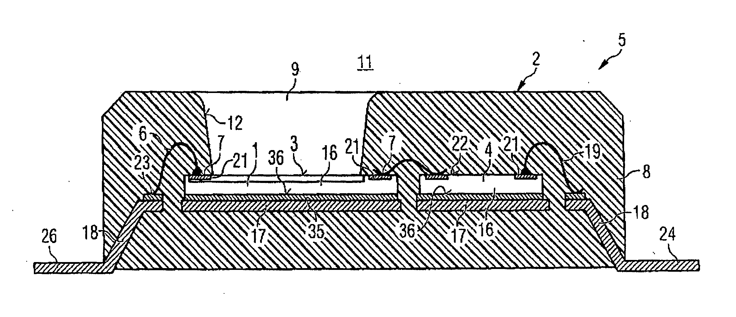
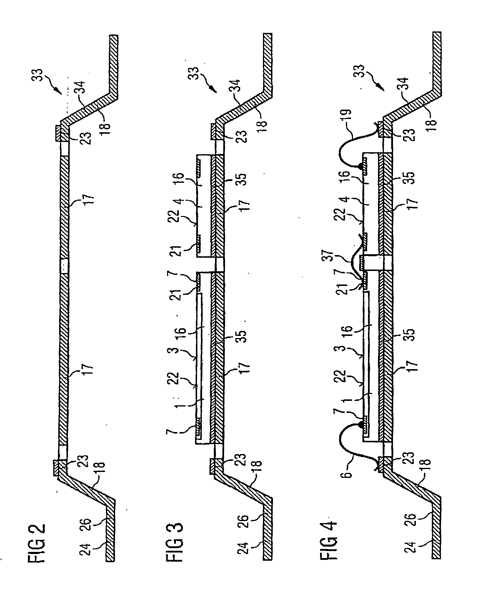
[0038]FIG. 1 shows a schematic cross section through a semiconductor module 5 according to a first embodiment of the invention. This semiconductor module 5 has a sensor chip 1 and a further component 4 in the form of a semiconductor chip, which are positioned on chip islands 17 of inner flat conductors 18. The components 16 are fixed by their back sides 36 with a material bond by a layer of solder 35 on the chip islands 17. Electrical connections 6 in the form of bonding wire connections 19 connect contact areas 21 of the active upper side 22 of the components 16 to contact terminal areas 23 on inner flat conductors 18.

[0039] The inner flat conductors 18 go over outwardly into outer flat conductors 24 and form external contacts 26. The components 16 of the semiconductor module 5, such as the semiconductor chips, the bonding wire connections 19, the inner flat conductors 18 and the chip islands 17, are embedded in a nontransparent plastic molding compound 8. Of the sensor chip 1, th...


PUM


Abstract

The invention relates to a semiconductor module with a semiconductor sensor chip and an associated method. The sensor chip has a sensor region, and nonsensitive regions of the sensor chip are embedded in a nontransparent plastic package molding compound. The sensor region of the sensor chip is operably coupled to the external surroundings of the module via an opening in the nontransparent plastic package molding compound. The opening in the molding compound is formed by laser ablation.

Description

REFERENCE TO RELATED APPLICATIONS [0001] This application claims the benefit of the priority date of German application DE 10 2004 027 094.5, filed on Jun. 2, 2004, the contents of which are herein incorporated by reference in their entirety. FIELD OF THE INVENTION [0002] The invention relates to a semiconductor module with a semiconductor sensor chip and a plastic package as well as to a method for its production. The sensor chip of this semiconductor module has a sensor region and is electrically in connection with at least one further component of the semiconductor module, with at least the further component embedded in a plastic molding compound. BACKGROUND OF THE INVENTION [0003] Semiconductor modules are known, for example, as disclosed in German patent application DE 103 30 739.7. In this known embodiment of a semiconductor module, although a semiconductor chip is embedded in a nontransparent plastic package molding compound, the entire sensor chip with its electrical connect...

Claims


Application Information

Patent Timeline
Patent Type & Authority Applications(United States)
IPC IPC(8): H01L31/0203B81B7/00
CPCB81B7/0067B81B2207/012H01L2924/01327H01L2924/1815H01L2224/73265H01L2224/48465H01L2224/48247H01L2224/32245H01L2924/01322H01L2924/01068H01L2224/48137H01L2924/01079H01L2924/00H01L2224/48472H01L2224/4945H01L2924/181H01L2924/00012
Inventor AUBURGER, ALBERTPAULUS, STEFANKOLLER, ADOLF
Owner AVAGO TECHNOLOGIED FIBER IP SINGAPORE PTE LTD
Why Eureka
Try Eureka