
Forming electrical conductors on a substrate

a technology of electrical conductors and substrates, applied in the direction of dielectric characteristics, light absorption dielectrics, instruments, etc., can solve the problems of substrate deformation, high cost, and difficult to achieve lateral dimensions less than 100 microns,

Inactive Publication Date: 2006-01-05
EASTMAN KODAK CO
View PDF15 Cites 31 Cited by
  • Summary
  • Abstract
  • Description
  • Claims
  • Application Information

AI Technical Summary

Benefits of technology

[0007] The invention and its objects and advantages will become more apparent in the detailed description of the preferred embodiment presented below.

Problems solved by technology

This method, however, is a high-cost operation and is only suitable for batch processing.
Some problems associated with this technique are that it is substrate dependent, it is difficult to achieve lateral dimensions of less than 100 microns, and the particles must be annealed by bulk heating, which can cause substrate deformation.
Another problem with inkjet deposition is that it often requires multiple passes to deposit the proper amount of material, which reduces throughput.
Gold nanoparticles, which are used as an example, have low absorption in the visible spectrum resulting in low heating efficiency.
This low heating efficiency is a problem in commercial applications because of low writing speeds.

Method used


Image

  • Forming electrical conductors on a substrate
  • Forming electrical conductors on a substrate
  • Forming electrical conductors on a substrate

Examples


Embodiment Construction

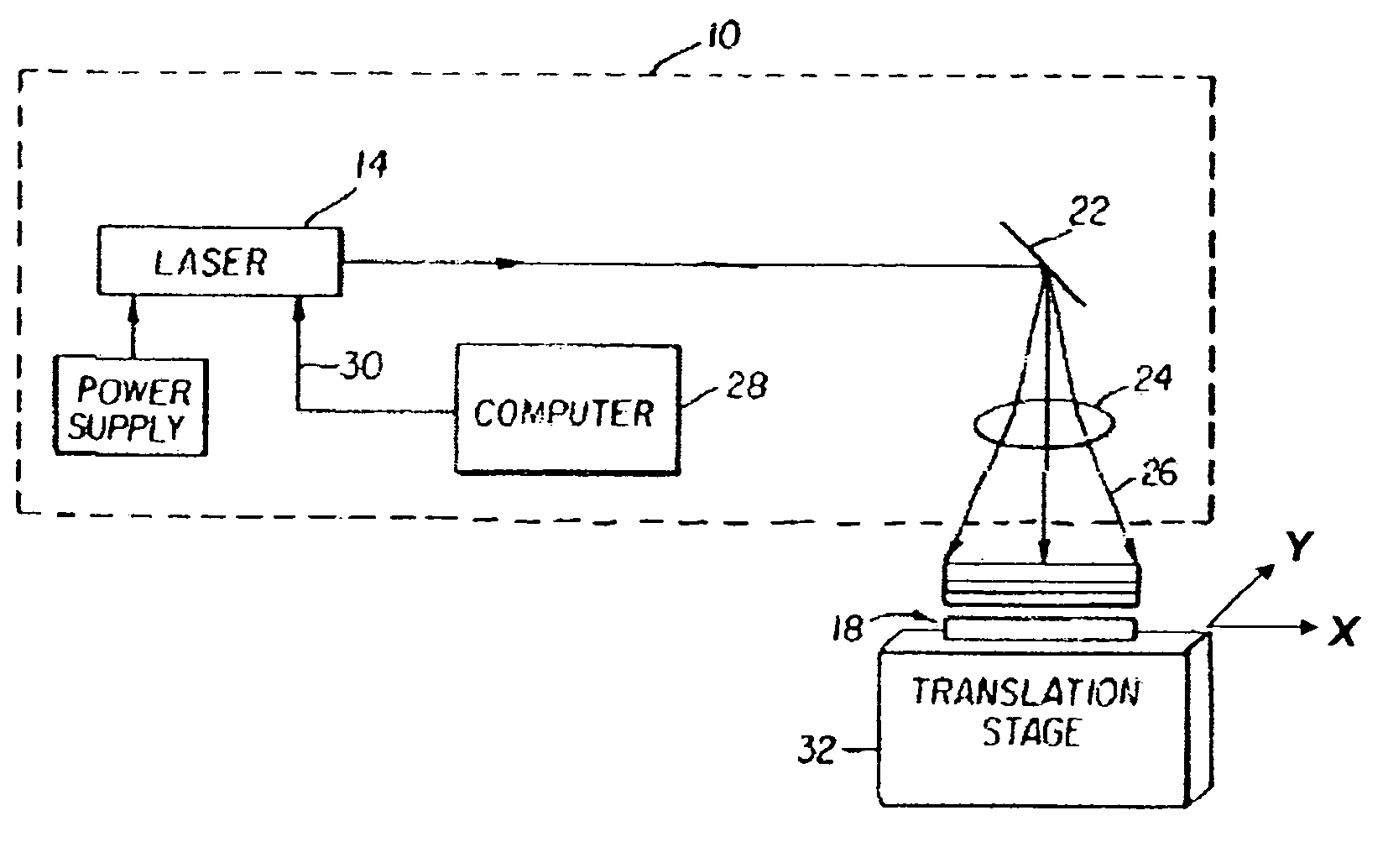
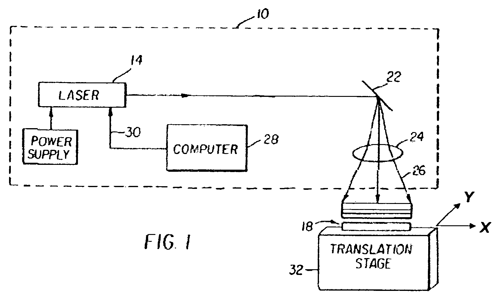
[0015] One of most characteristic feature of metal nanoparticles is the size-dependent surface melting point depression. (Ph. Buffat et al.; “Size effect on the melting temperature of gold particles” Physical Review A, Volume 13, Number 6, June 1976, pages 2287-2297; A. N. Goldstein et al.; “Melting in Semiconductor Nanocrystals” Science, Volume 256, Jun. 5, 1992, pages 1425-1427; and K. K. Nanda et al.; “Liquid-drop model for the size-dependent melting of low-dimensional systems” Physical Review, A 66 (2002), pages 013208-1 thru 013208-8.) This property would enable the melting or sintering of the metal nanoparticles into polycrystalline films with good electric conductivity. (D. Huang, et al.; “Plastic-Compatible Low Resistance Printable Gold Nanoparticle Conductors for Flexible Electronic” Journal of the Electrochemical Society, Volume 150, Issue 7, July 2003, Abstract.) The present invention will be directed to a method of forming a pattern of electrical conductors on a substrat...


PUM

PropertyMeasurementUnit
temperatureaaaaaaaaaa
thicknessaaaaaaaaaa

Abstract

A method of forming a pattern of electrical conductors on a substrate (18) consists of forming metal nanoparticles on a conductive material. A light absorbing dye is mixed with the metal nanoparticles. The mixture is then coated on the substrate. The pattern is formed on the coated substrate with laser light (14). Unannealed material is removed from the substrate.

Description

FIELD OF THE INVENTION [0001] The invention relates in general to forming a pattern of conductors on a substrate and in particular to forming conductors on a substrate by selectively annealing a mixture of laser light absorbing dyes and metal nanoparticles. BACKGROUND OF THE INVENTION [0002] It is often necessary to print large area electrical circuits with conductors having at least one lateral dimension of 1-1000 microns. One process for accomplishing this type of circuit printing is using vacuum deposition. This method, however, is a high-cost operation and is only suitable for batch processing. [0003] Another method of constructing electrical circuits is inkjet printing of patterns using metal nanoparticles to form conductors. This process is discussed in S. Molesa et al.; “High-quality inkjet-printed multilevel interconnects and inductive components on plastic for ultra-low-cost RFID applications.” University of California, Berkeley. Some problems associated with this technique...

Claims


Application Information

Patent Timeline
Patent Type & Authority Applications(United States)
IPC IPC(8): G03C5/00B44C1/22
CPCH05K3/02H05K3/102H05K2203/107H05K2201/0257H05K2201/0112
Inventor YANG, ZHIHAOKAY, DAVID B.TUTT, LEE W.
Owner EASTMAN KODAK CO
Learn More