Mask, substrate with light reflection film, manufacturing method for light reflection film, manufacturing method for electro-optical device, and electro-optical device, and electronic apparatus

a manufacturing method and technology of light reflection film, applied in the direction of mirrors, instruments, photomechanical treatment, etc., can solve the problems of affecting the display quality, so as to achieve uniform reflection characteristics, improve display quality, and facilitate manufacturing

Inactive Publication Date: 2006-01-12
BOE TECH GRP CO LTD
View PDF17 Cites 5 Cited by
  • Summary
  • Abstract
  • Description
  • Claims
  • Application Information

AI Technical Summary

Benefits of technology

[0016] That is, regarding liquid crystal display device, etc., using the substrate with light reflection film, by making dots a basic unit while the number of the dots is smaller than the number of the dot regions, for example, by arranging light transmission portions or light non-transmission portions in the direction of the plane on a random basis in units of 3 dots, 6 dots, or 12 dots of RGB dots corresponding to the pixel, the information content regarding the pattern formed from the light transmission portions or light non-transmission portions can be reduced. Consequently, when a desired pattern, for example, a pattern formed from the light transmission portions or the light non-transmission portions having the two-dimensional shapes of independent circles (hereafter, ellipses are included) and polygons, or of either of them, is formed, the design of the mask can be performed with remarkable ease in a short time by repetition of such a basic unit.
[0017] Since the light transmission portions or light non-transmission portions are arranged in the direction of the plane on a random basis, when the substrate with light reflection film is manufactured, excellent light scattering effect can be exhibited and occurrence of interference fringes can be prevented effectively.
[0023] According to this configuration, the substrate with light reflection film which brings about few interference fringes can be effectively manufactured. That is, since when the substrate with light reflection film is manufactured, it is possible to scatter light moderately by the use of a predetermined symmetrical pattern, for example, a pattern which is in mirror plane symmetry with respect to a virtual line with a mask divided by the virtual line, occurrence of interference fringes can be effectively prevented. Since the symmetrical pattern is used and the pattern is used repeatedly, the information content regarding the pattern can be reduced and, therefore, manufacture of the substrate with light reflection film becomes easy.
[0025] As described above, since the convex portions or the concave portions are arranged in the direction of the plane on a random basis in units of, for example, 3 dots, 6 dots, or 12 dots of RGB dots corresponding to the pixel, excellent light scattering effect can be exhibited and occurrence of interference fringes can be prevented effectively.
[0028] By specifying the heights of the plurality of convex portions or depths of the plurality of concave portions to be substantially the same as described above, manufacture can be performed with ease and, in addition, uniform reflection characteristics can be achieved.

Problems solved by technology

However, it is difficult to make the surface of such a protection plate facing the liquid crystal display device a perfectly smooth surface, and in many cases, fine concavities and convexities exist.
When such a protection plate was placed in the liquid crystal display device, there was a problem in that the display quality was degraded remarkably due to the fine concavities and convexities on the surface.
Causes of this degradation of the display quality include that the interval between the substrate and the protection plate on the observation side in the liquid crystal display device varies depending on the concavities and convexities existing on the surface of the protection plate.
That is, interference occurs when emitted light from the liquid crystal display device passes through the protection plate corresponding to the aforementioned variations in the intervals and, as a result, the interference fringes occur.
Consequently, it is assumed that the degradation of the display quality is brought about by overlapping of the interference fringes and the display image.
However, regarding liquid crystal display devices, for example, the reflective liquid crystal display and the reflection transmission combination (transflective) type liquid crystal display device disclosed in Japanese Unexamined Patent Application Publication No. 6-27481, etc., although the masks, in which a plurality of circles having different diameters, etc., have been regularly or partially irregularly arranged, have been used in order to place a plurality of concavity and convexity structures having different heights by the use of ultraviolet exposure and development, it has been difficult to precisely adjust the heights so as to effectively prevent interference of light because of variations in coating thicknesses, etc.
Furthermore, since the reflection electrode has been formed on the plurality of concavity and convexity structures having different heights, there have been problems in that breaks and short circuits have been likely to occur, and the like.
Regarding the disclosed manufacturing method for the substrate with light reflection film, there have been problems relating to manufacture in that a large number of steps have been required and many items have been required to control.
Therefore, regarding the substrates with light reflection film described in Japanese Unexamined Patent Application Publication No. 6-27481, etc., it has been difficult to effectively prevent the occurrence of the interference fringes and, in addition, it has been difficult to stably and efficiently manufacture such a substrate with light reflection film.

Method used


Image

  • Mask, substrate with light reflection film, manufacturing method for light reflection film, manufacturing method for electro-optical device, and electro-optical device, and electronic apparatus
  • Mask, substrate with light reflection film, manufacturing method for light reflection film, manufacturing method for electro-optical device, and electro-optical device, and electronic apparatus
  • Mask, substrate with light reflection film, manufacturing method for light reflection film, manufacturing method for electro-optical device, and electro-optical device, and electronic apparatus

Examples


first embodiment

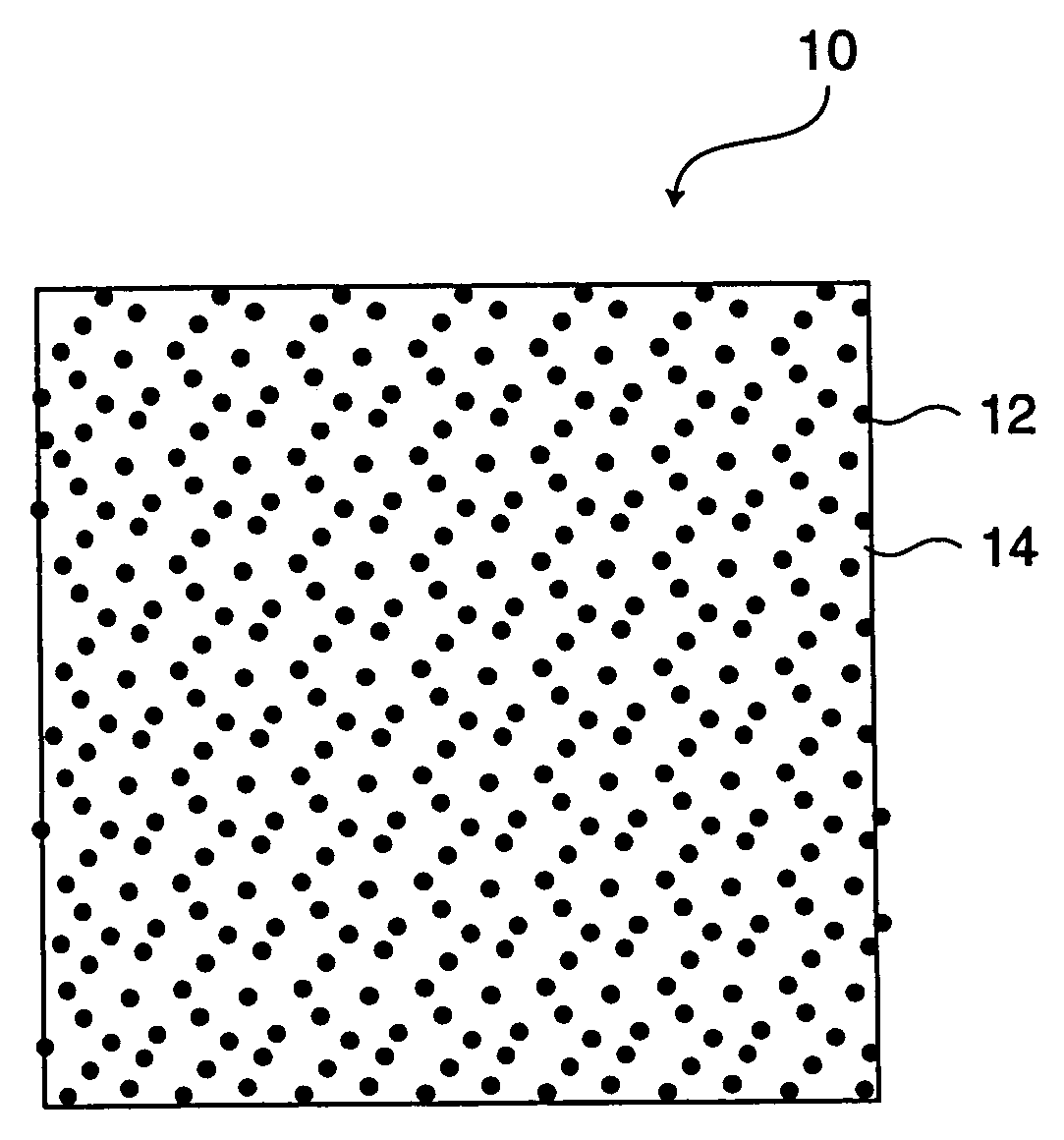
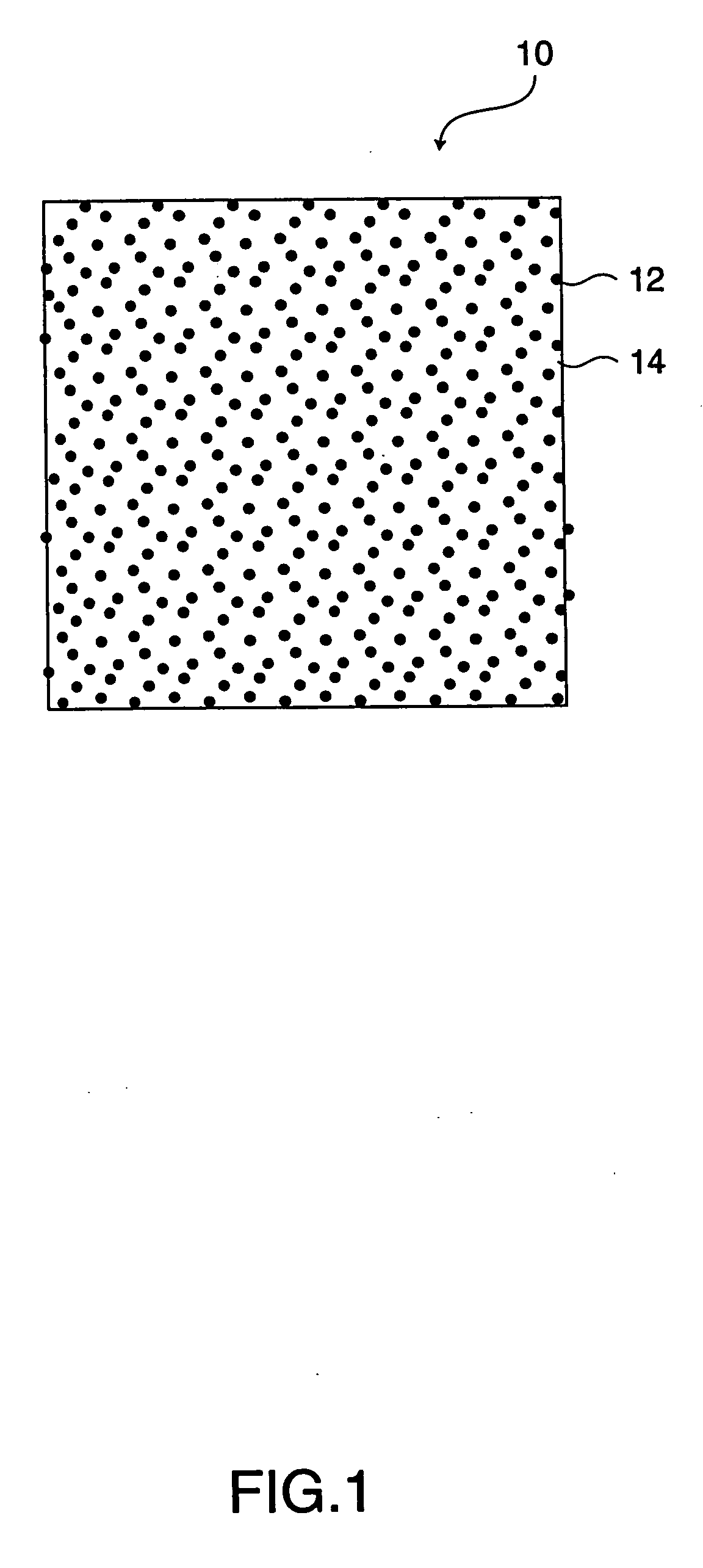
[0086] The first embodiment is a mask for forming a pattern on a substrate including a plurality of dot regions, provided with light transmission portions which can transmit incident light and light non-transmission portions which, substantially, do not transmit light, wherein a pattern formed from the light transmission portions or light non-transmission portions is formed in units of dots, the number thereof being smaller than the number of the dot regions, and has an irregular arrangement in each of the units, and a plurality of units are included.

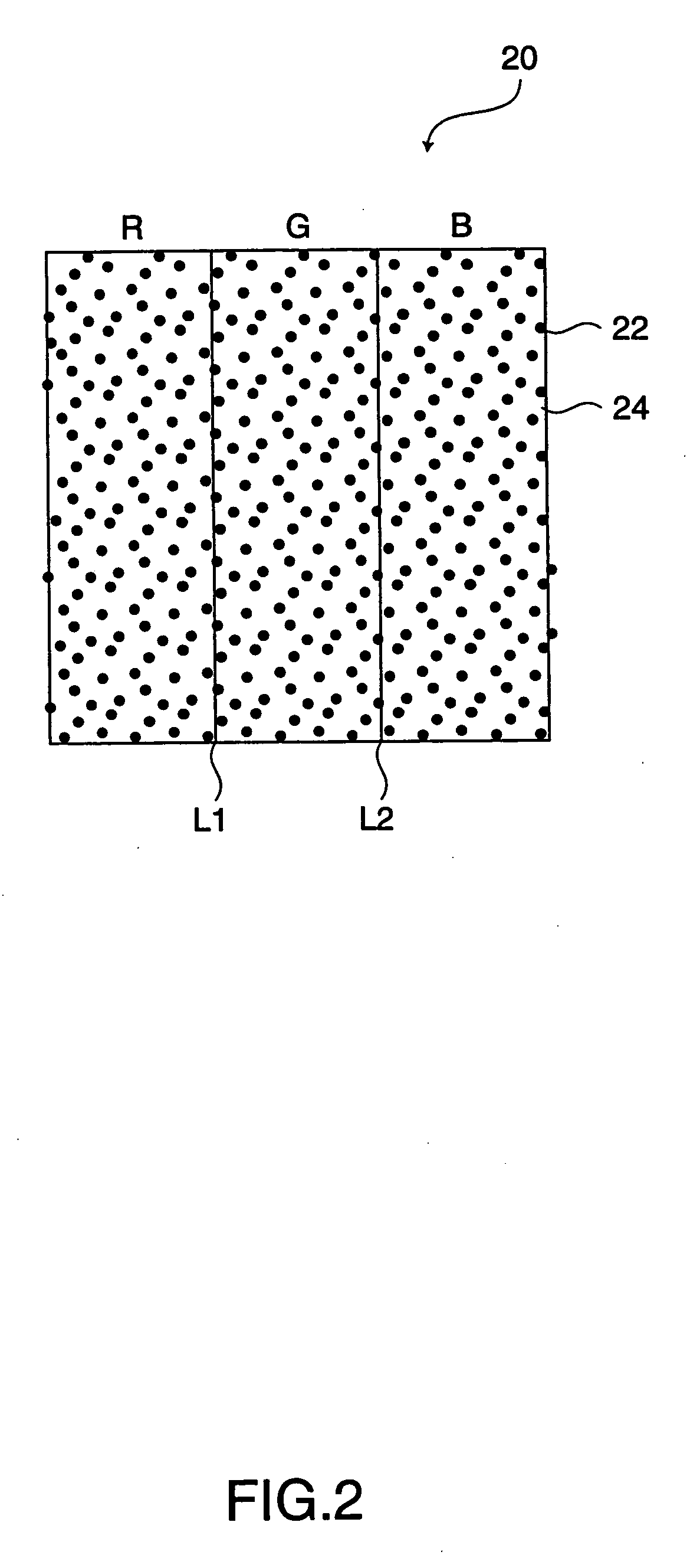
[0087] That is, for example, the mask is a mask 20 as shown in FIG. 2 for manufacturing a substrate with light reflection film, wherein light transmission portions or light non-transmission portions 22 have the two-dimensional shapes of independent circles and polygons, or of either of them, and are arranged in the direction of the plane on a random basis in units of RGB dots corresponding to the predetermined pixel.

[0088] Light Trans...

second embodiment

[0127] The second embodiment is a substrate with light reflection film, in which a light reflection film is formed on a substrate including a plurality of dot regions, wherein the light reflection film having convex portions or concave portions is included, and a pattern formed from the convex portions or concave portions has an irregular arrangement in each unit defined by a plurality of dots.

[0128] That is, in the case shown in FIG. 7 as an example, where a negative type photosensitive resin is used, a substrate 70 with light reflection film includes a base material 77 and a reflection layer 72, the heights of a plurality of convex portions 76 or the depths of a plurality of concave portions formed on the base material 77 are specified to be substantially the same, the two-dimensional shapes of the plurality of convex portions 76 are specified to be the two-dimensional shapes of independent circles and polygons, or of either of them, and the plurality of convex portions 76 are ar...

third embodiment

[0176] The third embodiment is a manufacturing method for forming a light reflection film on a base material including a plurality of dot regions, provided with a step of coating the base material with a photosensitive material, a step of exposing the photosensitive material, a step of forming concavities and convexities on the photosensitive material exposed, and a step of forming a light reflection film on the concavities and convexities. A pattern of the concavities and convexities is formed in units of a plurality of dots fewer than the number of the dot regions and has an irregular arrangement in each of the units.

[0177] That is, the manufacturing method for the substrate with light reflection film includes a step for forming a first base material including a plurality of convex portions or concave portions having substantially the same height, which are arranged in the direction of the plane on a random basis and which are independent of each other, by the exposure process wi...


PUM

PropertyMeasurementUnit
hazeaaaaaaaaaa
hazeaaaaaaaaaa
diametersaaaaaaaaaa

Abstract

A substrate is provided with a light reflection film in which the heights of a plurality of convex portions or the depths of concave portions formed on a base material are specified to be substantially the same. The two-dimensional shapes of the plurality of convex portions or concave portions are specified to be the two-dimensional shapes of independent circles and polygons, or of either of them. In addition, the plurality of convex portions or concave portions are arranged in the direction of the plane on a random basis. The substrate is formed using a mask in which light transmission portions or light non-transmission portions are formed in units of dots, the number thereof being smaller than the number of dot regions. The dots are arranged irregularly in each of the units, and a plurality of units are included.

Description

CROSS REFERENCE TO RELATED APPLICATIONS [0001] This application is a divisional patent application of U.S. Ser. No. 10 / 175,344 filed Jun. 19, 2002, claiming priority to Japanese Patent Application Nos. 2002-108526 filed Apr. 10, 2002 and 2001-186694 filed Jun. 20, 2001 all of which are hereby incorporated by reference.BACKGROUND OF THE INVENTION [0002] 1. Technical Field of the Invention [0003] The present invention relates to a mask, a substrate with a light reflection film, a manufacturing method for a light reflection film, a manufacturing method for an electro-optical device, and an electro-optical device, and an electronic apparatus. [0004] For further details, the present invention relates to a mask for producing a substrate with light reflection film which brings about few interference fringes, a substrate with light reflection film using the same, a manufacturing method for a light reflection film, and an electro-optical device provided with the substrate with light reflecti...

Claims


Application Information

Patent Timeline
Patent Type & Authority Applications(United States)
IPC IPC(8): G02F1/29G02B5/02G02B5/08G02B5/20G02F1/1335G02F1/13363G02F1/167G03F1/52G03F1/68
CPCG02F1/133553G02B5/201G02F1/13363
Inventor OTAKE, TOSHIHIROMATSUO, MUTSUMITSUYUKI, TADASHI
Owner BOE TECH GRP CO LTD
Why Eureka
Try Eureka