Method for manufacturing semiconductor physical quantity sensor

Inactive Publication Date: 2006-01-12
DENSO CORP
View PDF7 Cites 8 Cited by
  • Summary
  • Abstract
  • Description
  • Claims
  • Application Information

AI Technical Summary

Benefits of technology

[0013] The above method provides the physical quantity sensor with high manufac

Problems solved by technology

Further, design degree of freed

Method used


Image

  • Method for manufacturing semiconductor physical quantity sensor
  • Method for manufacturing semiconductor physical quantity sensor
  • Method for manufacturing semiconductor physical quantity sensor

Examples


first embodiment

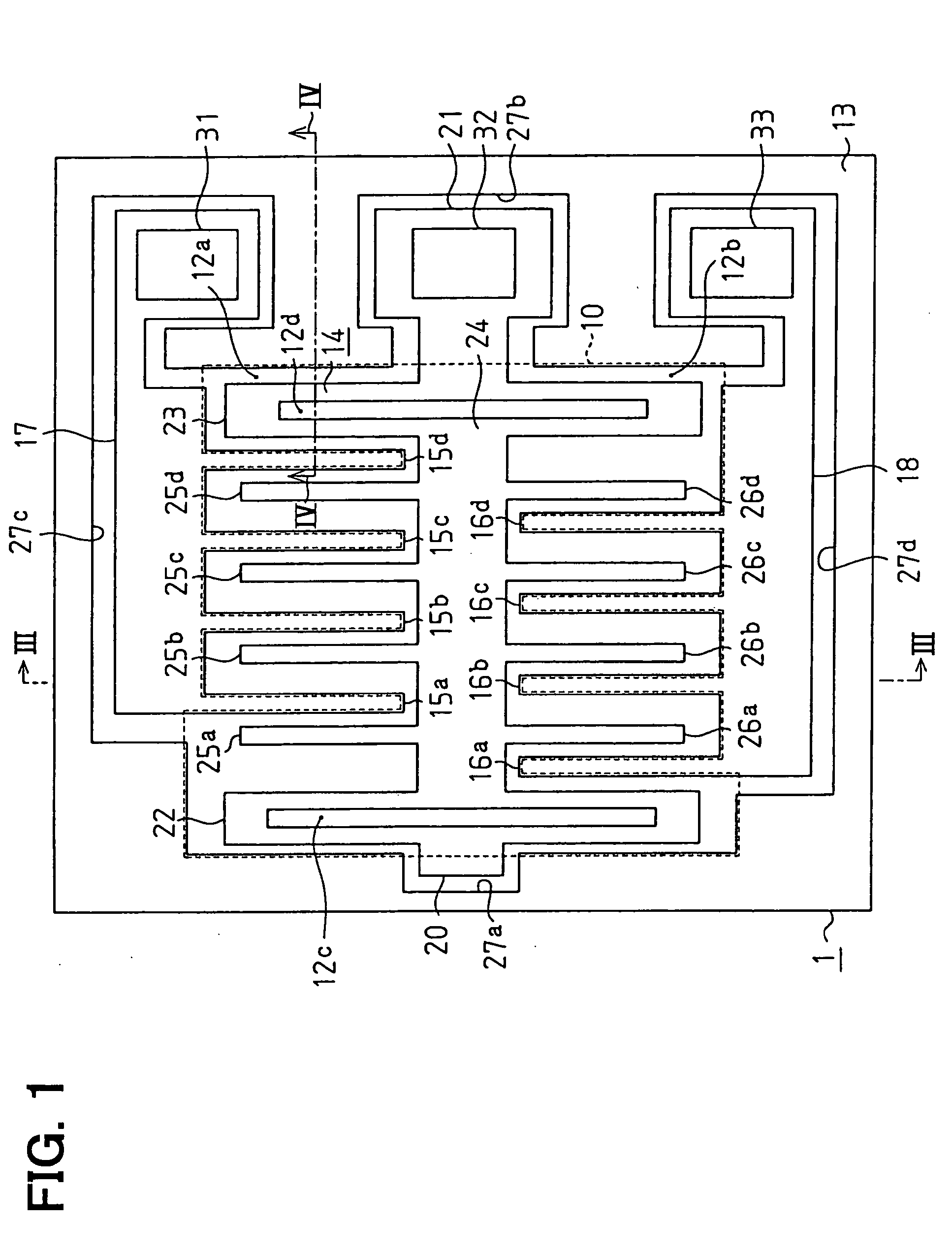
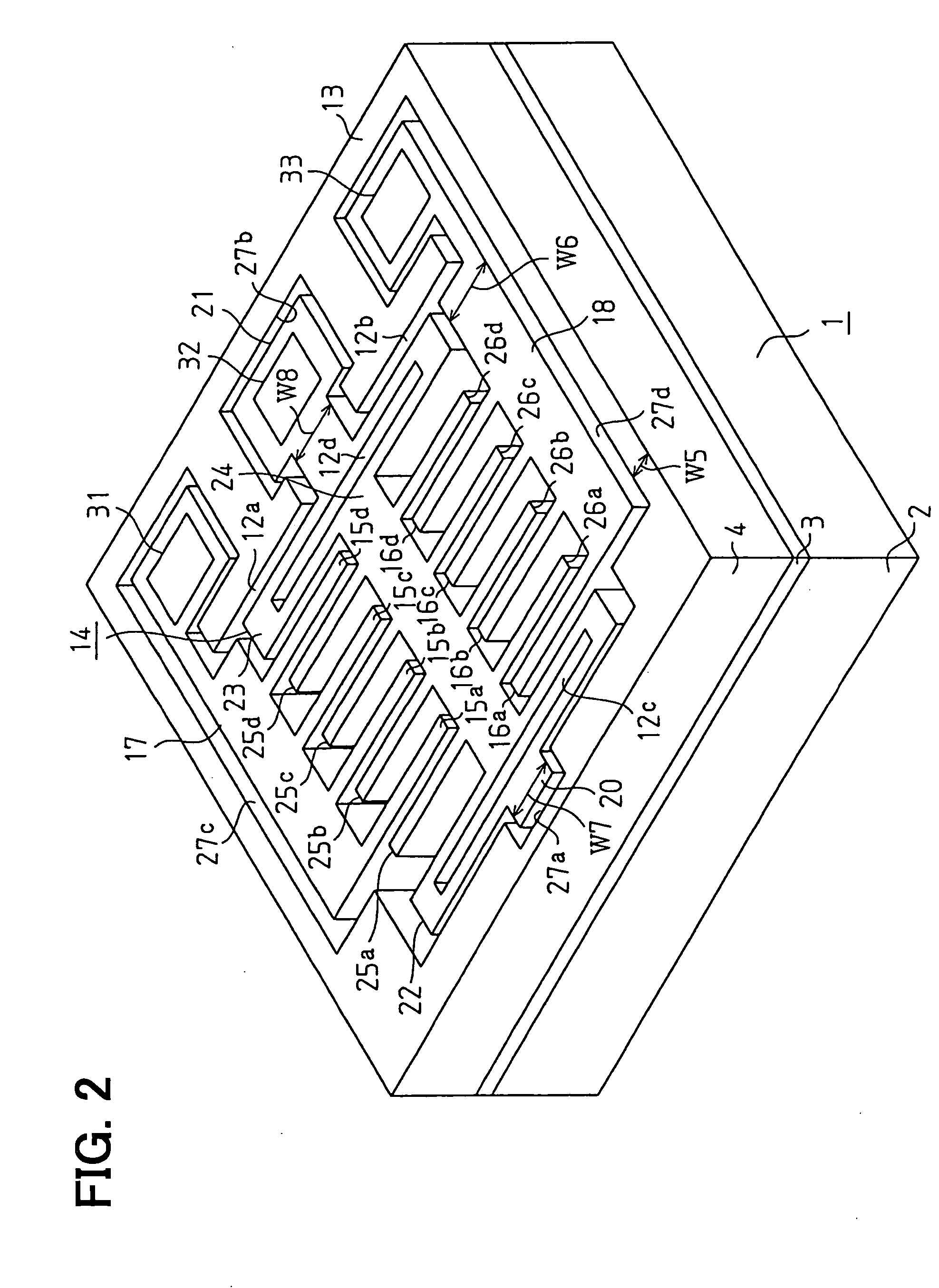
[0045] A semiconductor physical quantity sensor according to a first embodiment of the present invention is shown in FIGS. 1 to 3. The sensor is an acceleration sensor. In FIG. 3, the sensor is manufactured by a multi-layered substrate 1, which is made of a SOI substrate. The substrate 1 includes a silicon substrate 2, an embedded insulation film 3 and a silicon layer 4, which are stacked in this order. The embedded insulation film 3 is made of a silicon nitridefilm (i.e., a SiN film). A cavity 10 is formed in the silicon layer 4 of the substrate 1. The cavity 10 has a predetermined height of T1. The cavity 10 extends in a horizontal direction (i.e., a lateral direction) of the substrate 1. A formation region of the cavity 10 is shown as a broken line in FIG. 1.

[0046] Multiple grooves 12a-12d are formed in the silicon layer 4, and disposed over the cavity 10. These grooves 12a-12d extend in a vertical direction of the substrate 1. Further, the grooves 12a-12d reach the cavity 10. O...

second embodiment

[0069] A semiconductor acceleration sensor according to a second embodiment of the present invention is shown in FIG. 15. FIG. 15 is a cross section of the sensor taken along line IV-IV in FIG. 1.

[0070] The sensor includes the silicon substrate 2, the embedded insulation film 3 and the silicon layer 4, which are stacked in this order so that the multi-layered substrate 1 is formed. Here, the cavity 10 is disposed under the movable portion such as the beam 23, and the embedded insulation film 3 is disposed under the fixed portion such as the fixed electrode 15d.

[0071] The method for manufacturing the sensor is described as follows. As shown in FIG. 17, the multi-layered substrate 1 having the embedded insulation film 3 as a sacrifice layer is prepared. The embedded insulation film 3 is made of a silicon oxide film. Specifically, as shown in FIG. 16, the first substrate 101 having a silicon oxide film 120 disposed on the substrate 101 is prepared. Further, the second substrate 110 h...

third embodiment

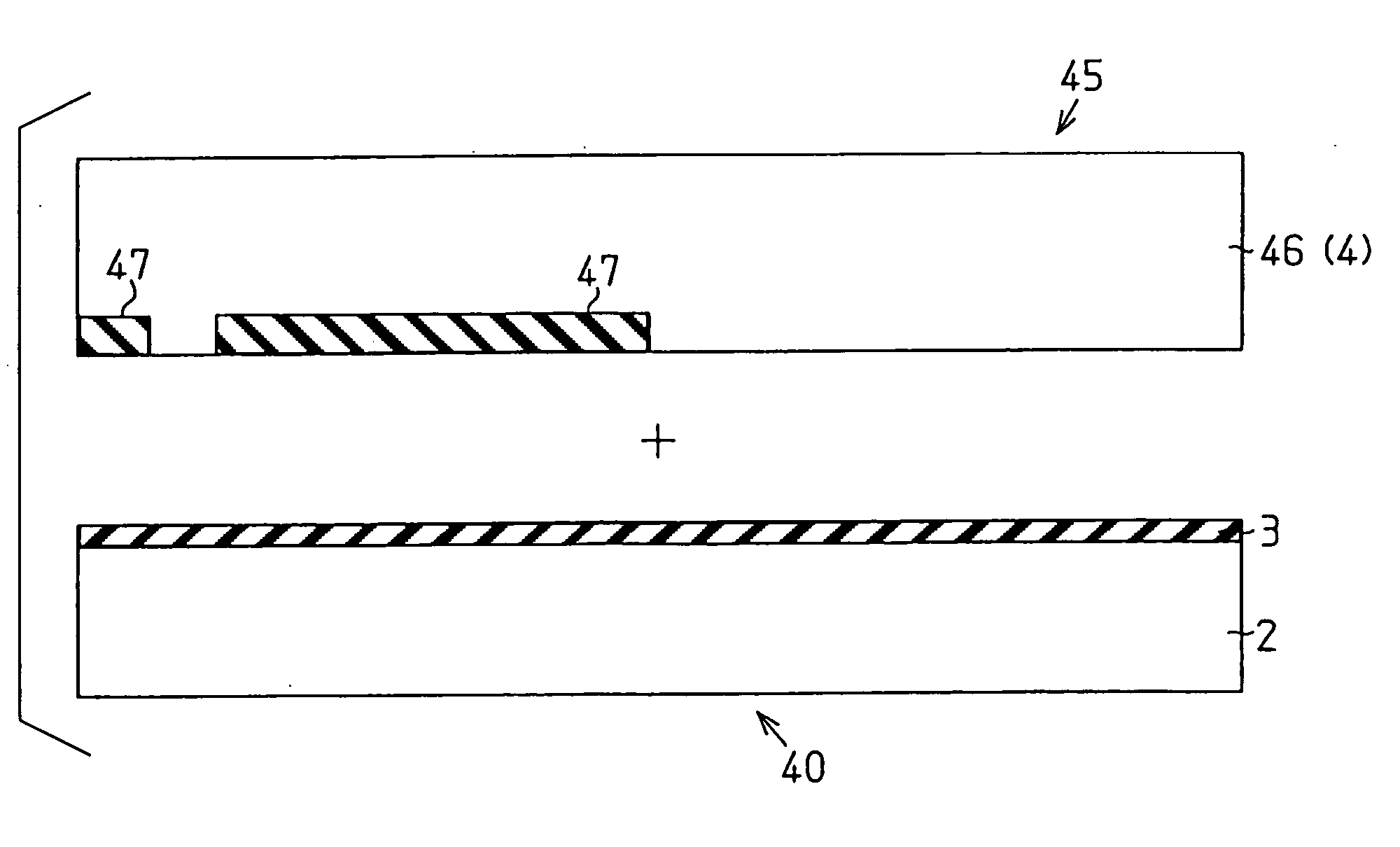
[0074] A physical quantity sensor according to a third embodiment of the present invention is shown in FIGS. 20-22. The sensor includes a silicon nitride film 300 as a protection layer. The silicon nitride film 300 covers the embedded insulation film 3 made of a silicon oxide film so that the embedded insulation film 3 is protected from etching when the sacrifice oxide film 47 is removed.

[0075] The method for manufacturing the sensor is shown in FIGS. 23 to 25B. The first substrate 40 includes the silicon substrate 2, the embedded insulation film 3 and the silicon nitride film 300. The silicon nitride film 300 is formed on the embedded oxide film 3. The first and the second substrates 40, 45 are bonded each other in such a manner that the silicon nitride film 300 of the first substrate 40 is bonded to the sacrifice oxide film 47 of the second substrate 45. As shown in FIG. 25A, when the cavity 10 is formed by removing the sacrifice oxide film 47, the silicon nitride film 300 protec...


PUM


Abstract

A method for manufacturing a semiconductor physical quantity sensor is provided. The sensor includes a multi-layered substrate, a cavity, a groove, a movable portion and a fixed portion. The multi-layered substrate includes a support substrate, an embedded insulation film, and a semiconductor layer. The method includes the steps of: preparing the multi-layered substrate having a sacrifice layer embedded in the semiconductor layer so that the sacrifice layer is disposed at a cavity-to-be-formed portion; forming the groove from the semiconductor layer to reach the sacrifice layer; and selectively etching the sacrifice layer from a bottom of the groove to form a cavity.

Description

CROSS REFERENCE TO RELATED APPLICATIONS [0001] This application is based on Japanese Patent Applications No. 2004-199739 filed on Jul. 6, 2004, and No. 2005-160600 filed on May 31, 2005, the disclosures of which are incorporated herein by references. FIELD OF THE INVENTION [0002] The present invention relates to a method for manufacturing a semiconductor physical quantity sensor. BACKGROUND OF THE INVENTION [0003] A physical quantity sensor having a beam structure formed in a semiconductor substrate is disclosed in, for example, Japanese Patent Application Publication No. H06-349806. The beam structure is formed in the substrate by a micro machining method. As shown in FIG. 19A, a SOI substrate having a silicon substrate 200, an embedded oxide film 201 and a silicon layer 202 is prepared. The silicon layer 202 is formed on the silicon substrate 200 through the embedded oxide film 201. A groove 210 is formed in the silicon layer 202. The groove 210 extends in a vertical direction of ...

Claims


Application Information

Patent Timeline
IPC IPC(8): H01L21/00H01L21/30
CPCB81B2201/0292B81B2203/0118G01P2015/0814G01P15/0802G01P15/125B81C1/00142
Inventor ASAI, MAKOTO
Owner DENSO CORP
Why Eureka
Try Eureka