Check patentability & draft patents in minutes with Patsnap Eureka AI!

Carbon nanotube field emitter and method for producing same

a carbon nanotube and emitter technology, applied in the field of field emitters, can solve the problems of researchers and manufacturers, no related experiments or data supporting the achievements of this patent, and the support of the patent claims of the patent is not supported, so as to achieve the effect of simple and low-cost manufacturing process

Inactive Publication Date: 2006-01-19
TAI NYAN HWA +2
View PDF9 Cites 3 Cited by
  • Summary
  • Abstract
  • Description
  • Claims
  • Application Information

AI Technical Summary

Benefits of technology

"The present invention provides a simple and low-cost manufacturing process to make an electrode using carbon nanotube as the electron emitter source. The method involves producing a substrate with highly integrated internal circuits using a low-temperature co-fire ceramic sintering process, screen printing a carbon nanotube paste onto the substrate to form at least one emitter source, heat treating the product, and sintering the product. The resulting field emission carbon nanotube emitter has a highly integrated ceramic substrate and an emitter source formed on it, which can emit a plurality of electrons when a voltage is applied. The technical effects of this invention are a simplified and cost-effective process for manufacturing a highly efficient carbon nanotube emitter."

Problems solved by technology

However, the technological claims of this patent have not been supported by related experiment data yet.
Although the U.S. Pat. No. 6,146,230 proposed a simple and low-cost manufacturing process, no related experiments or data supports its achievements.
Therefore, one of the difficult topics for researchers and manufacturers to overcome is to develop a simple manufacturing process with low costs for producing high performce electrode.

Method used


Image

  • Carbon nanotube field emitter and method for producing same
  • Carbon nanotube field emitter and method for producing same
  • Carbon nanotube field emitter and method for producing same

Examples


Embodiment Construction

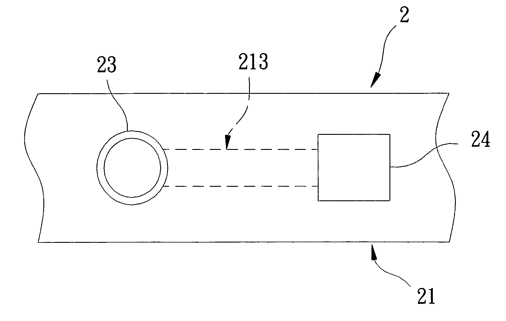
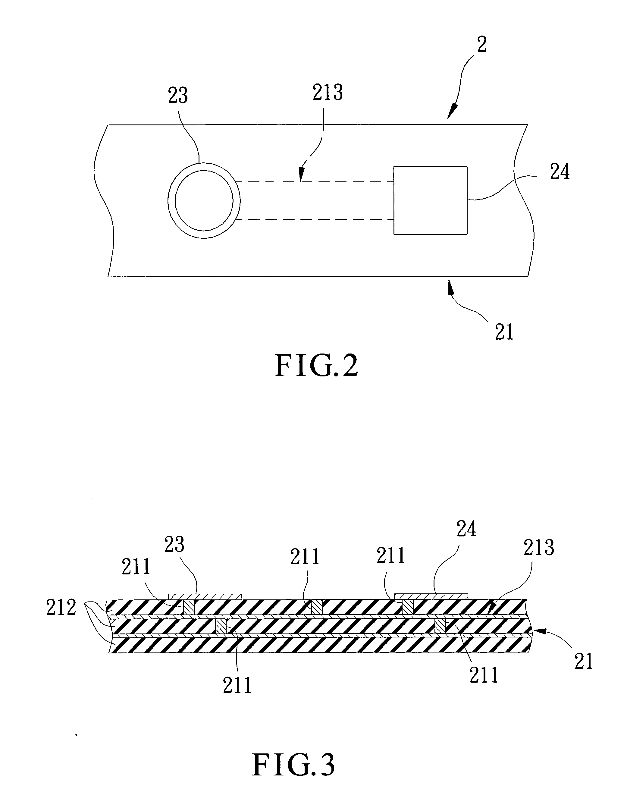
[0030] Referring to FIG. 1 for a method for producing a carbon nanotube electrode according to a preferred embodiment of the present invention, the carbon nanotube electrode 2 so produced as shown in FIG. 2 can be used for a field emitting display or a light emitting device, etc.

[0031] In the meantime, referring to FIGS. 2 and 3 for the carbon nanotube electrode 2, which comprises a ceramic substrate 21, an electrode unit 24 formed on the ceramic substrate 21 and an emitter source 23 formed on the ceramic substrate 21.

[0032] The ceramic substrate 21 is an integrated ceramic substrate comprising at least two vias 211 for an electrical connection and an internal circuit 213 formed between two ceramic tapes 212 and a plurality of vias 211. The internal circuit also can be substituted by adopting a conductive layer produced by an electrically conductive material.

[0033] The electrode base 24 is produced by an electrically conductive material such as a silver paste and electrically con...


PUM

PropertyMeasurementUnit
diameteraaaaaaaaaa
diameteraaaaaaaaaa
particle diameteraaaaaaaaaa

Abstract

A carbon nanotube electrode includes a plurality of carbon nanotubes as the electron emitter. The manufacturing method involves the preparation of a carbon nanotube paste, screen printing circuits onto a substrate for forming integrated circuits after sintering, screen printing a carbon nanotube with the carbon nanotube paste onto the substrate to form an emitter source, and going through a thermal treatment process and a sintering process to obtain a good-quality carbon nanotube electrode with a threshold voltage lower than 1.9 V / μm.

Description

BACKGROUND OF THE INVENTION [0001] 1. Field of the Invention [0002] The present invention relates to a field emitter, more particularly to a field electrode that uses a carbon nanotube as the emitter source and its manufacturing method. [0003] 2. Description of the Related Art [0004] In general, various materials including metal spindts and thin diamond films used for field emitters require a very high threshold field (i.e. the electric field required for the current density of Je=10 mA / cm2) before accomplishing good performance. Many technical literatures and journals have shown that better performance can be obtained if the carbon nanotube is applied to field emitters. It shows that the carbon nanotube is an excellent material for manufacturing field emitters. [0005] At present, the field emitter using carbon nanotubes as an electron emitter source is generally produced by growing carbon nanotubes directly on a substrate and then adding appropriately designed components to form th...

Claims


Application Information

Patent Timeline
Patent Type & Authority Applications(United States)
IPC IPC(8): H01J1/14
CPCB82Y10/00H01J2201/30469H01J9/025H01J1/304
Inventor TAI, NYAN-HWALIN, I-NANTSAI, TSUNG-YEN
Owner TAI NYAN HWA
Features
  • R&D
  • Intellectual Property
  • Life Sciences
  • Materials
  • Tech Scout
  • Unparalleled Data Quality
  • Higher Quality Content
  • 60% Fewer Hallucinations
Learn More