Light-emitting device and electronic apparatus

a technology of light-emitting devices and electronic devices, which is applied in the direction of discharge tubes/lamp details, wing accessories, discharge tubes luminescnet screens, etc., can solve the problems of increased manufacturing process complexity, reduced display contrast, and deterioration of contrast, so as to suppress manufacturing costs, improve display contrast, and suppress light reflection

Inactive Publication Date: 2006-01-19
SEIKO EPSON CORP
View PDF7 Cites 13 Cited by
  • Summary
  • Abstract
  • Description
  • Claims
  • Application Information

AI Technical Summary

Benefits of technology

[0007] An advantage of the invention is that it provides a light-emitting device which is capable of suppressing light reflection at a wiring line or a cathode without complicating a manufacturing process to improve display contrast and to suppress manufacturing costs, and an electronic apparatus having the light-emitting device mounted therein.
[0008] According to a first aspect of the invention, there is provided a light-emitting device including a transparent substrate, a light-emitting layer which is provided on one surface of the substrate and which emits light in response to an electrical signal, a conductive portion which transmits the electrical signal to the light-emitting layer, such that light from the light-emitting layer is emitted after being transmitted through the substrate, and a light transflective layer which is provided between the conductive portion and the substrate at a predetermined distance from the conductive portion to reflect some of incident light through the substrate and to transmit the remainder.
[0009] In this case, some of incident light transmitted through the substrate is reflected by the light transflective layer and the remainder is reflected by the conductive portion after being transmitted through the light transflective layer and returns to the light transflective layer. Therefore, by setting a distance between the light transflective layer and the conductive portion to the predetermined distance, light reflected by the light transflective layer and light reflected by the conductive portion interfere with each other to cancel out. Accordingly, when the light-emitting device is driven, since light reflected from the conductive portion is not recognized, the contrast can be improved. In addition, since the light transflective layer may be formed on the portion on which the conductive portion is formed, it is not necessary to perform patterning to cover the regions between the wiring lines. Further, it is not necessary to use a circularly polarizing plate. Therefore, the light-emitting device can be manufactured at low cost without complicating a manufacturing process.
[0010] In addition, various transparent insulating members may be provided between the light transflective layer and the conductive portion. The materials may be freely selected. Further, when the member, such as the black matrix, for absorbing light is arranged, converted heat may be accumulated in the corresponding light absorbing member to have a bad influence on the light-emitting device. However, according to the invention, the light transflective layer is arranged, so that light interferes with each other to cancel out. Accordingly, heat is not accumulated and thus the light-emitting device can be stably driven. In particular, when the invention is applied to the organic EL device, it is possible to drive the light-emitting device without having the bad influence on the light-emitting layer.
[0011] In this case, it is preferable that ‘the predetermined distance’ be a distance that light reflected by the light transflective layer and light reflected by the conductive portion interfere with each other to cancel out, for example, a distance at which a zero-order interference occurs. However, in a case in which the light transflective layer and the conductive portion are arranged to be excessively adjacent to each other and it is difficult to interpose the insulating member therebetween, the determined distance may be a distance at which a first-order interference or a second-order interference occurs. In addition, since ‘some’ and ‘the remainder’ of incident light mean ‘some’ and ‘the remainder’ of the intensity or amount of incident light, not ‘some’ and ‘the remainder’ of wavelength components.
[0012] It is preferable that the light transflective layer have substantially the same pattern as that of the conductive portion. In this case, the pattern of the light transflective layer may be formed such that the shape thereof is equal to that of the conductive portion. As a result, when the conductive portion and the light transflective layer are manufactured, the same process may be repeated, and it is not necessary that a specific manufacturing process be performed. In addition, the light transflective layer may be formed larger than the conductive portion. As a result, for example, it is possible to transmit and reflect light from an oblique direction and thus it is possible to further improve the contrast.

Problems solved by technology

As a result, the contrast may be deteriorated.
However, since the circularly polarizing plate is expensive, the cost of a light-emitting device using the circularly polarizing plate increases.
Further, in the method disclosed in Japanese Unexamined Patent Application Publication No. 10-214043, it is necessary to pattern the black matrix so as to cover the regions between wiring lines and thus the manufacturing process is complex.
Further, when the member, such as the black matrix, for absorbing light is arranged, converted heat may be accumulated in the corresponding light absorbing member to have a bad influence on the light-emitting device.
However, in a case in which the light transflective layer and the conductive portion are arranged to be excessively adjacent to each other and it is difficult to interpose the insulating member therebetween, the determined distance may be a distance at which a first-order interference or a second-order interference occurs.

Method used


Image

  • Light-emitting device and electronic apparatus
  • Light-emitting device and electronic apparatus
  • Light-emitting device and electronic apparatus

Examples


first embodiment

(First Embodiment)

[0040] A first embodiment of the invention will now be described with reference to the accompanying drawings. In the accompanying drawings, the scales of respective elements are suitably changed so that the elements can be clearly recognized.

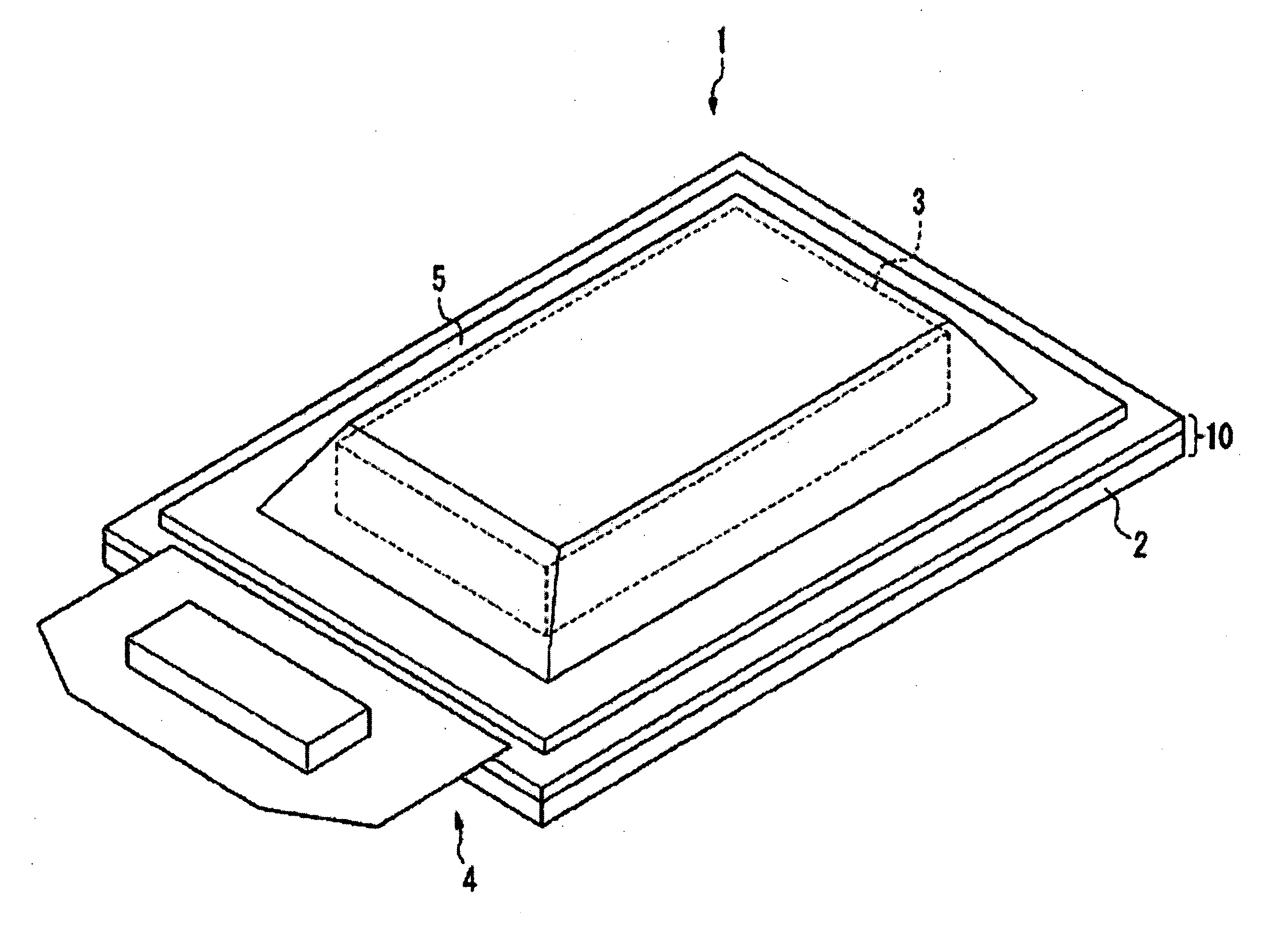
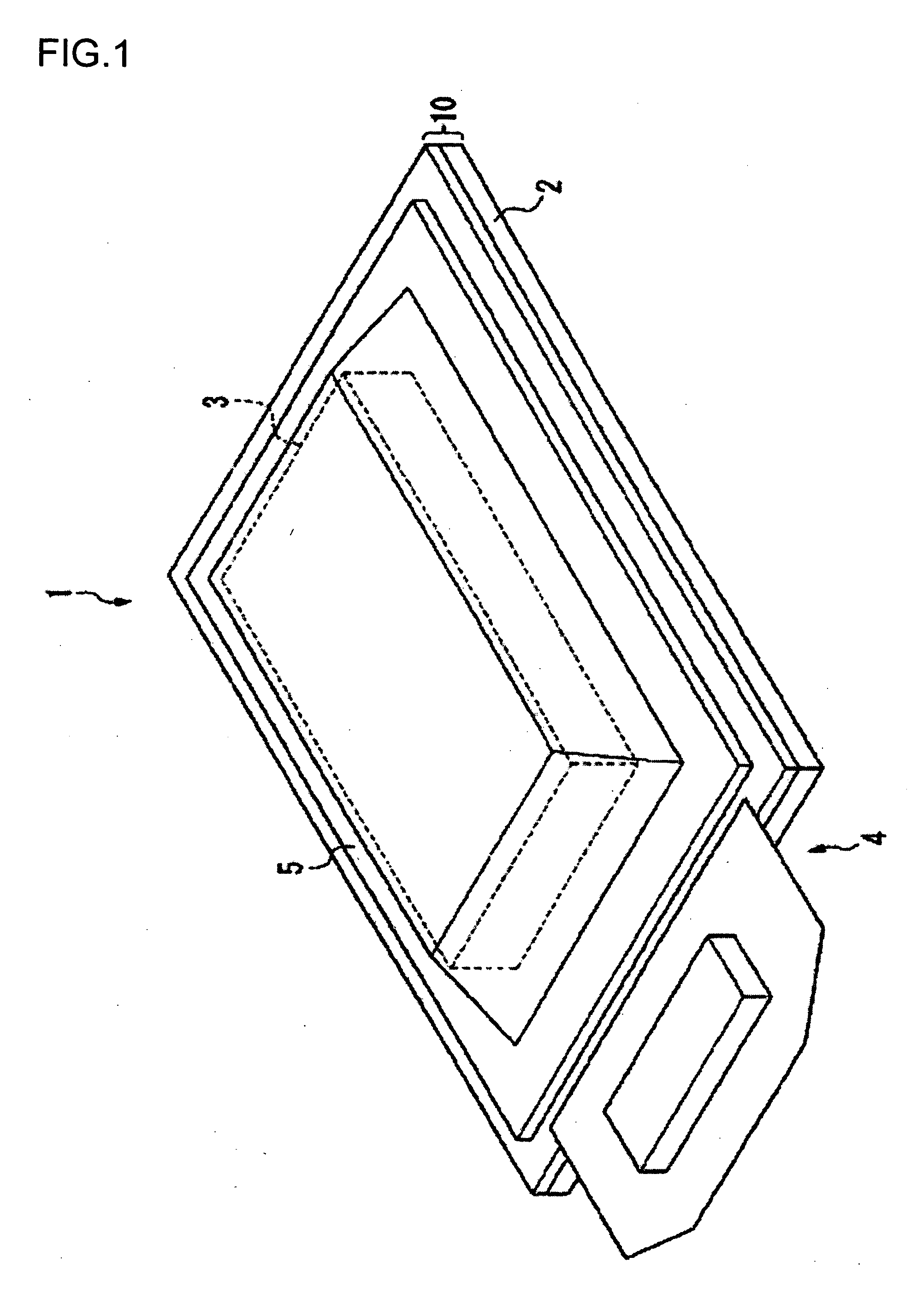
[0041]FIG. 1 is a perspective view schematically showing the overall configuration of an organic EL device 1.

[0042] The organic EL device 1 includes a base substrate 10 having circuit elements or wiring lines, an insulating layer, and the like formed on a substrate 2, an organic EL element 3 formed on the base substrate 10, and an external circuit unit 4 attached to an end of the base substrate 10. The organic EL element 3 emits light according to an electrical signal which is supplied from the external circuit unit 4, such that an image or a moving picture is displayed. In addition, a sealing member 5 is provided to cover the organic EL element 3 and the base substrate 10. The organic EL device 1 exemplified in the present e...

second embodiment

(Second Embodiment)

[0084] Next, a second embodiment of the invention will be described. Similarly to the first embodiment, in the following drawings, the scales of the elements are suitably changed so that the elements can be clearly recognized. In addition, the same elements as those of the first embodiment are represented by the same reference numerals and the descriptions thereof will be omitted. In the present embodiment, since the configuration of the half mirror is different from that of the first embodiment, the present embodiment will be described with laying emphasis on this difference.

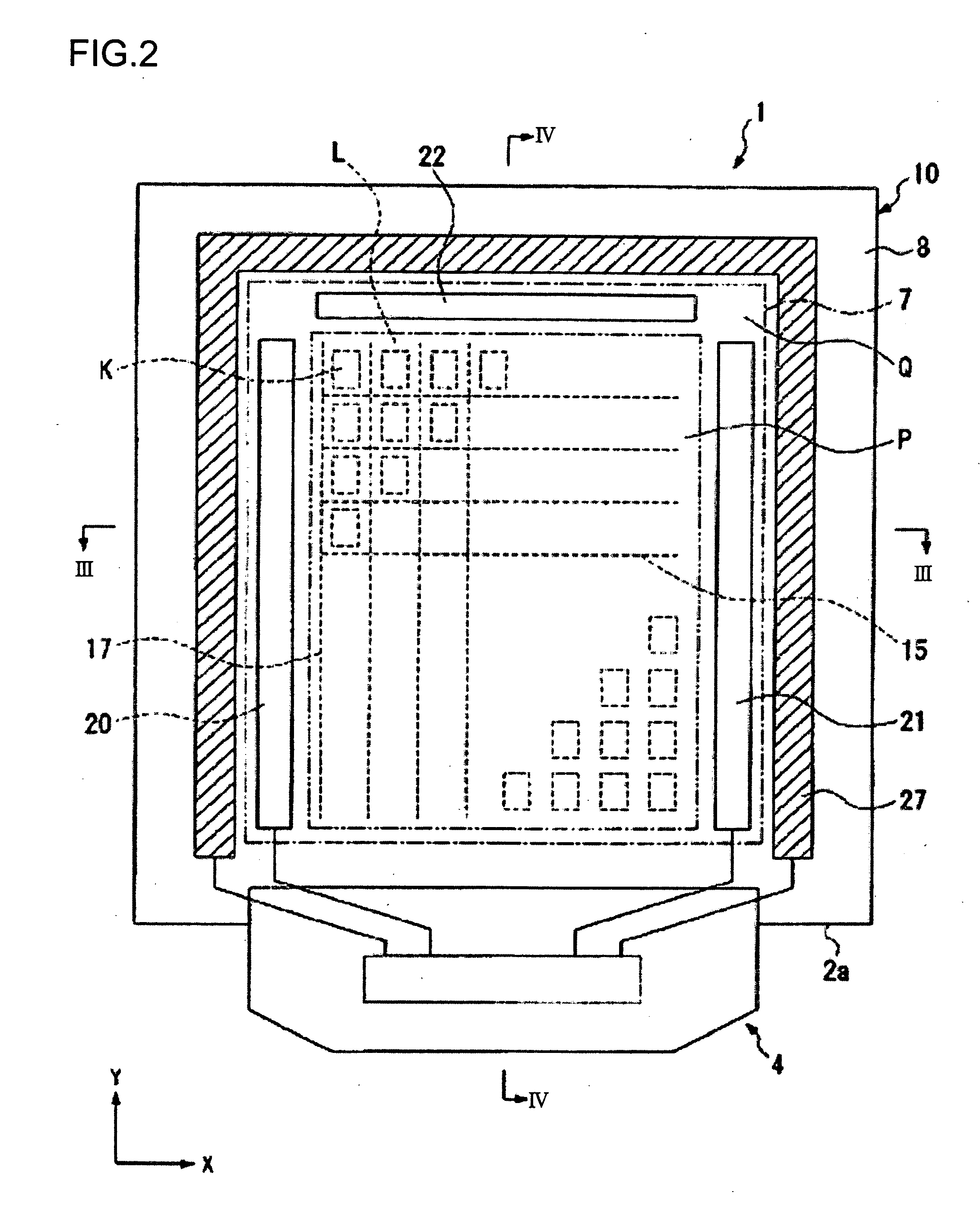
[0085]FIG. 9 is a schematic diagram showing the cross-section of an organic EL device 200 according to the second embodiment of the invention.

[0086] The organic EL device 200 includes a base substrate 10 in which circuit elements or wiring lines and an insulating layer formed on a substrate 2, an organic EL element 3 formed on the base substrate 10, and an external circuit unit 4 attached t...


PUM


Abstract

A light-emitting device includes a transparent substrate, a light-emitting layer which is provided on one surface of the substrate and which emits light in response to an electrical signal, a conductive portion which transmits the electrical signal to the light-emitting layer, such that light from the light-emitting layer is emitted after being transmitted through the substrate, and a light transflective layer which is provided between the conductive portion and the substrate at a predetermined distance from the conductive portion to reflect some of incident light through the substrate and to transmit the remainder.

Description

BACKGROUND OF THE INVENTION [0001] 1. Technical Field [0002] The invention relates to a light-emitting device such as an organic EL (electroluminescent) device or an inorganic EL device and to an electronic apparatus having the light-emitting device mounted therein. [0003] 2. Related Art [0004] In a bottom emission-type organic EL device, a plurality of light-emitting elements (pixels) are arranged on one surface of a transparent substrate, such as a glass substrate, with an insulating film provided therebetween. Further, wiring lines are formed on regions between pixels. Light generated at each pixel is emitted after being transmitted through the substrate. The substrate may transmit light emitted from a light-emitting layer to an exterior and allow light from the exterior to be incident on the inside of the organic EL device. In the inside of the organic EL device, ratio of areas between the light-emitting portion and the remaining portion other than the light-emitting portion in ...

Claims


Application Information

Patent Timeline
Patent Type & Authority Applications(United States)
IPC IPC(8): H05B33/00
CPCH01L51/5281H01L27/3244H10K59/12H10K50/86E05D15/48E05D15/063E06B3/5054E06B3/4636E05Y2201/688E05Y2201/684E05Y2900/132E05D2015/485
Inventor KOBAYASHI, HIDEKAZU
Owner SEIKO EPSON CORP
Why Eureka
Try Eureka