Layered ceramic electronic part and manufacturing method thereof

Active Publication Date: 2006-01-19
MURATA MFG CO LTD
View PDF5 Cites 13 Cited by
  • Summary
  • Abstract
  • Description
  • Claims
  • Application Information

AI Technical Summary

Benefits of technology

[0015] In accordance with various preferred embodiments of the present invention, by setting the porosity of the ceramic layer of the first element portion to be different from the porosity of the ceramic layer of the second element portion, even if the ceramic layer of the first element portion and the ceramic layer of the second element portion are made of the same materia

Problems solved by technology

Furthermore, in order to obtain satisfactory bonding, the magnetic layers and the nonmagnetic intermediate layer must be adjusted to have the same shrinkage rate during firing, which requires troublesome processes and techniques.
Furthe

Method used


Image

  • Layered ceramic electronic part and manufacturing method thereof
  • Layered ceramic electronic part and manufacturing method thereof
  • Layered ceramic electronic part and manufacturing method thereof

Examples


second preferred embodiment

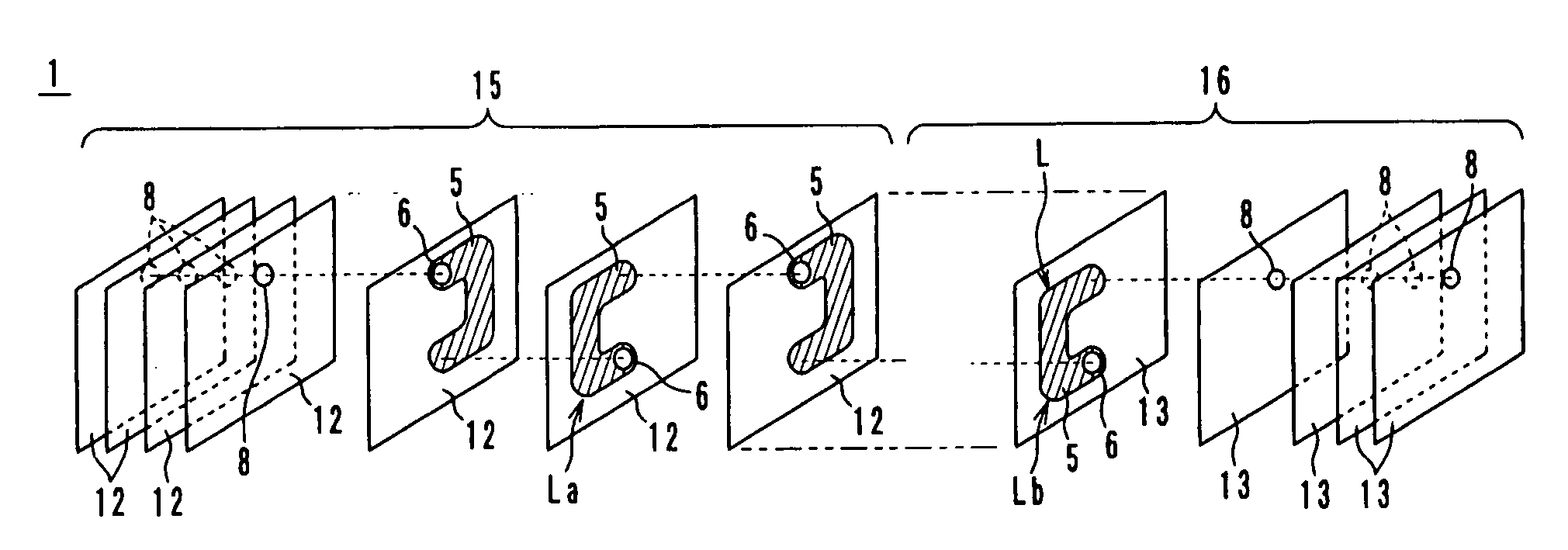
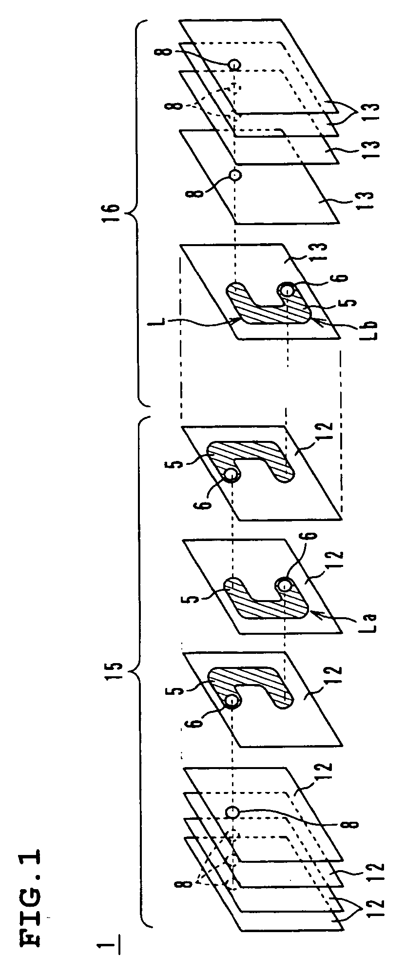
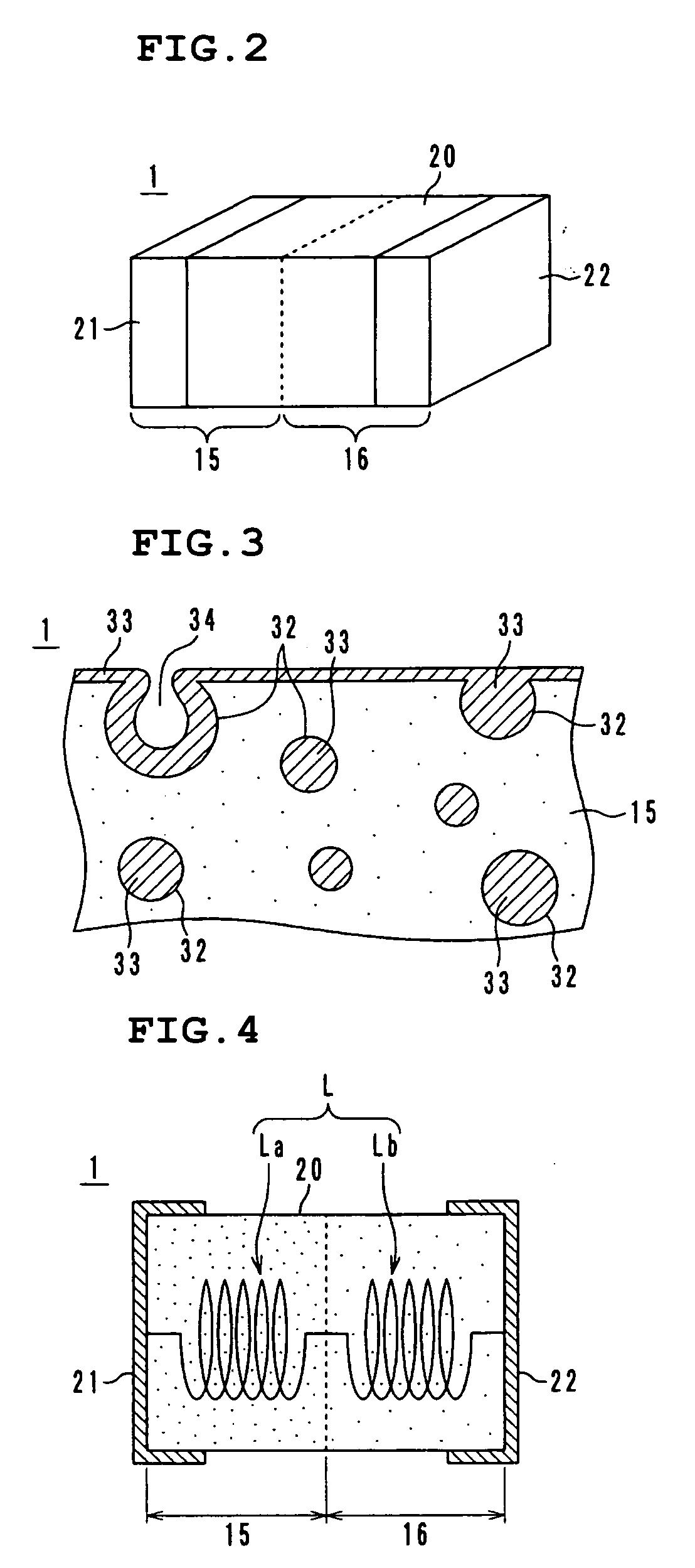
[0054] A second preferred embodiment is a monolithic inductor preferably having substantially the same structure as that of the first preferred embodiment. The high-permeability ceramic green sheet and the low-permeability ceramic green sheet are formed as in the first preferred embodiment using the same materials and by the same process except that a pore-forming agent is incorporated into the ferrite material when the high-permeability ceramic green sheet is formed, and the high-permeability coil portion has a porosity of about 20%. The low-permeability ceramic green sheet is formed as in the first preferred embodiment, and the low-permeability coil portion has a porosity of about 60%.

[0055] According to the second preferred embodiment, the same advantages as that of the first preferred embodiment are obtained, and since the pore-forming agent is incorporated into both the high-permeability coil portion and the low-permeability coil portion, the shrinkage rates during firing of t...


PUM


Abstract

A monolithic ceramic electronic component includes a low-permeability coil portion formed by stacking low-permeability ceramic green sheets, a first coil and a relatively large number of pores, and a high-permeability coil portion formed by stacking high-permeability ceramic green sheets, a second coil and a relatively small number of pores. The first coil and the second coil are electrically connected in series to form a spiral coil. The coil portion composed of a ferrite ceramic having a small number of pores has a high permeability and a high dielectric constant, and the coil portion composed of a ferrite ceramic having a large number of pores has a low permeability and a low dielectric constant.

Description

BACKGROUND OF THE INVENTION [0001] 1. Field of the Invention [0002] The present invention relates to monolithic ceramic electronic components and methods for making the same. More particularly, the present invention relates to monolithic ceramic electronic components, such as monolithic inductors, monolithic capacitors, and monolithic LC composite components, and methods for making the same. [0003] 2. Description of the Related Art [0004] In conventional noise suppression chip components, in order to ensure high impedance in the wide frequency range so that a noise reduction effect is achieved, for example, a component is fabricated by stacking a high-permeability magnetic layer and a low-permeability magnetic layer with a coil being disposed in each layer, and connecting the coils in series. [0005] As an example of such a component, Patent Document 1, Japanese Unexamined Patent Application Publication No. 9-7835, discloses a monolithic inductor having a structure in which a high-pe...

Claims


Application Information

Patent Timeline
IPC IPC(8): H01L21/00H01F17/00H01G4/40H03H7/075
CPCH01F17/0013H01F2017/002H01F2017/0026H03H2001/0085H03H7/075H03H2001/0057H01G4/40H01G4/232
Inventor TAKAZAWA, TOMOO
Owner MURATA MFG CO LTD
Why Eureka
Try Eureka