

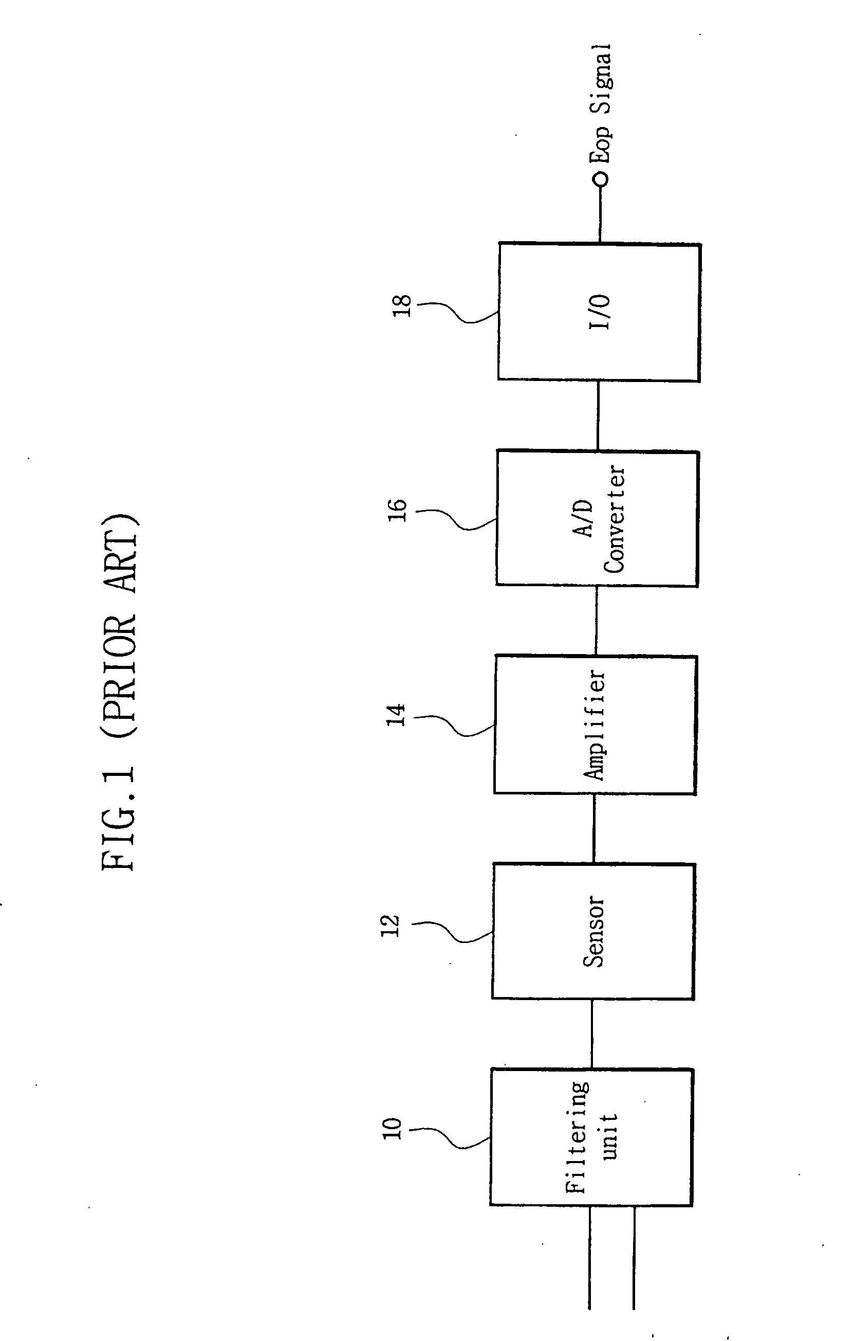
Endpoint detecting device in semiconductor manufacturing system
a semiconductor manufacturing system and endpoint detection technology, applied in the direction of semiconductor/solid-state device testing/measurement, electric discharge tubes, thermal excitation analysis, etc., can solve the uneven thickness of a material film between unit regions, the less widely used wet etch process, and the etch process. achieve the effect of improving the filter structur
- Summary
- Abstract
- Description
- Claims
- Application Information
AI Technical Summary
Benefits of technology
Problems solved by technology
Method used
Image

Examples
Embodiment Construction
[0035] The present invention will now be described more fully with reference to the accompanying drawings, in which preferred embodiments of the present invention are shown. The present invention may, however, be embodied in different forms and should not be construed as limited to only the embodiments set forth herein. Rather, these embodiments are provided as teaching examples of the present invention. Like numbers in the drawings refer to like elements.
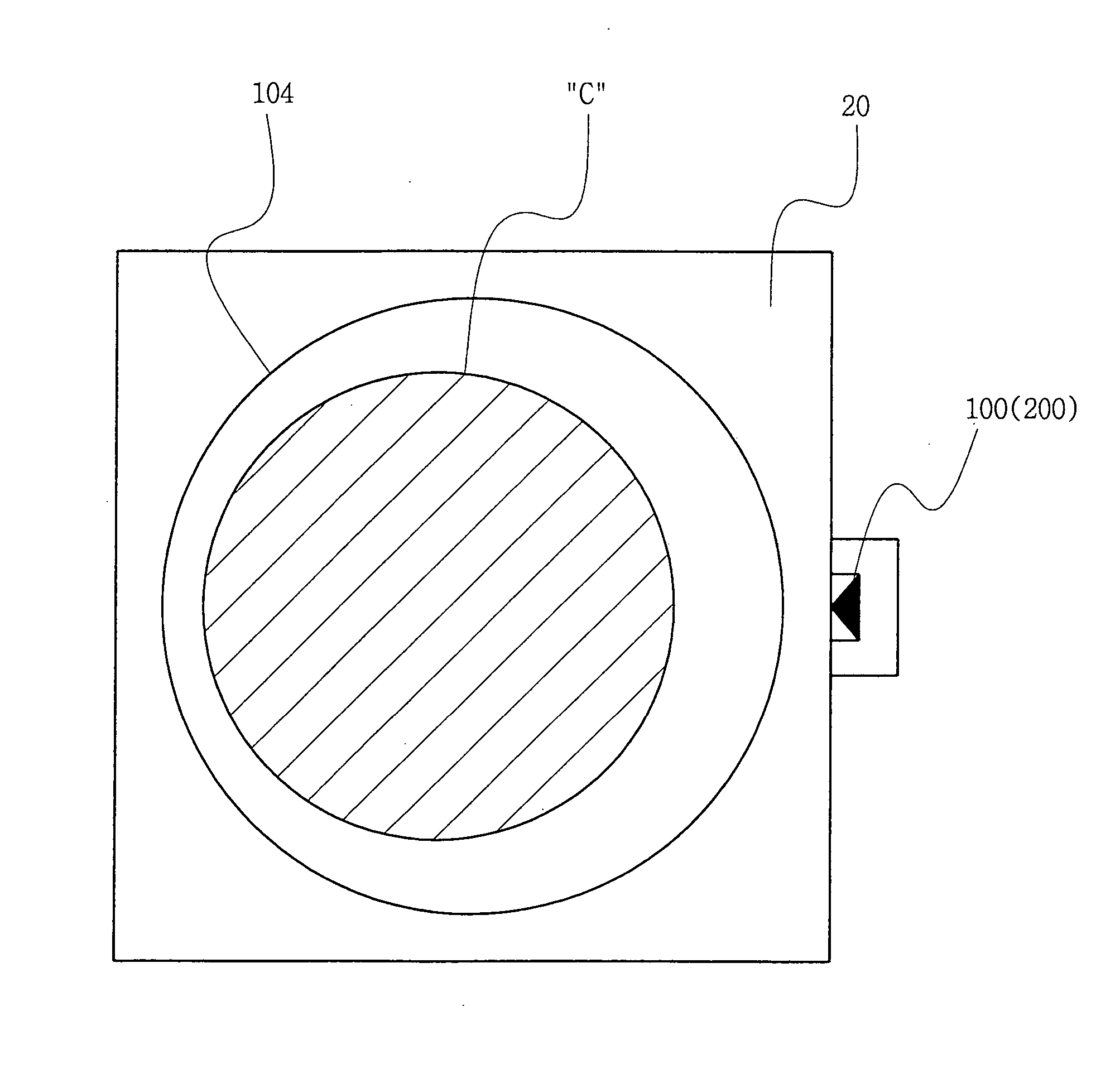
[0036]FIG. 4 is a view illustrating a filtering unit for an endpoint detecting device according to one embodiment of the present invention.
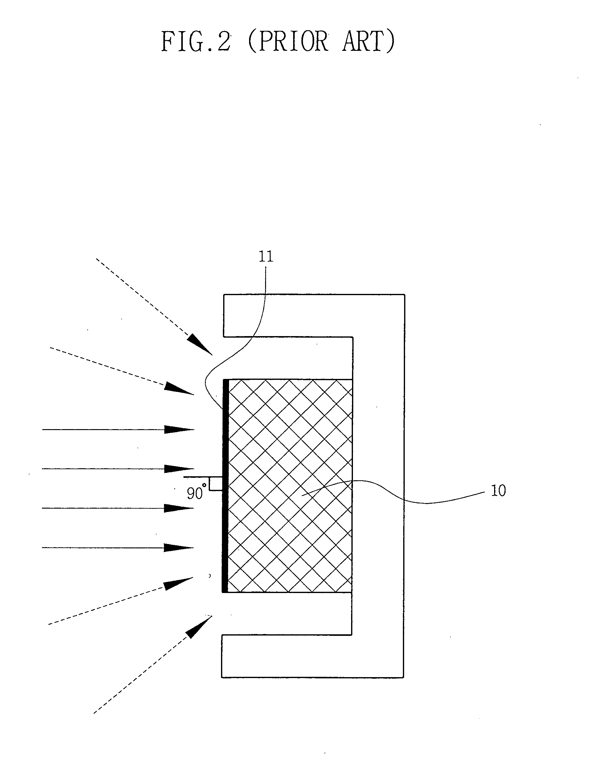
[0037] Referring to FIG. 4, a filter 100 has a polyhedron structure rather than the flat planar structure of the prior art. Filter 100 has at least two incidence surfaces 101 and 102. More specifically, filter 100 illustrated in FIG. 4 has a triangular prism shape. However, filter 100 may have various other polyhedron shapes such as a triangular pyramid, a quadrangular pyramid (pyramid structu...
PUM
| Property | Measurement | Unit |
|---|---|---|
| wavelength | aaaaa | aaaaa |
| wavelengths | aaaaa | aaaaa |
| plasma wavelengths | aaaaa | aaaaa |
Abstract
Description
Claims
Application Information