Dynamic deep depletion field effect transistor

a field effect transistor and deep depletion technology, applied in the field of trench-type fet, can solve problems such as increasing devices, and achieve the effect of high blocking voltag

Active Publication Date: 2006-01-26
INFINEON TECH AMERICAS CORP
View PDF4 Cites 52 Cited by
  • Summary
  • Abstract
  • Description
  • Claims
  • Application Information

AI Technical Summary

Benefits of technology

[0008] The gates may be simultaneously pulsed or alternately pulsed with voltages that allow the deep depletion to form. This device takes advantage of the known phenomenon that the depletion region at a MOS gate extends momentarily (tens of milliseconds) well beyond Wd at the threshold voltage.
[0009] For example: for 2E16 cm-3 epi doping level, the depletion w

Problems solved by technology

This low body concentration, however, i

Method used


Image

  • Dynamic deep depletion field effect transistor
  • Dynamic deep depletion field effect transistor
  • Dynamic deep depletion field effect transistor

Examples


Embodiment Construction

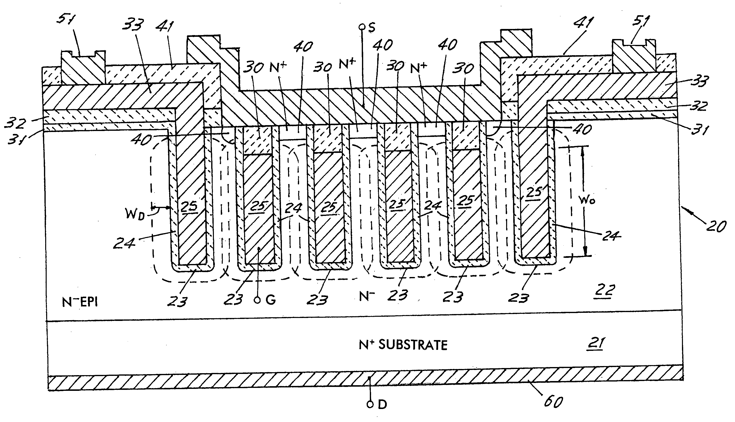
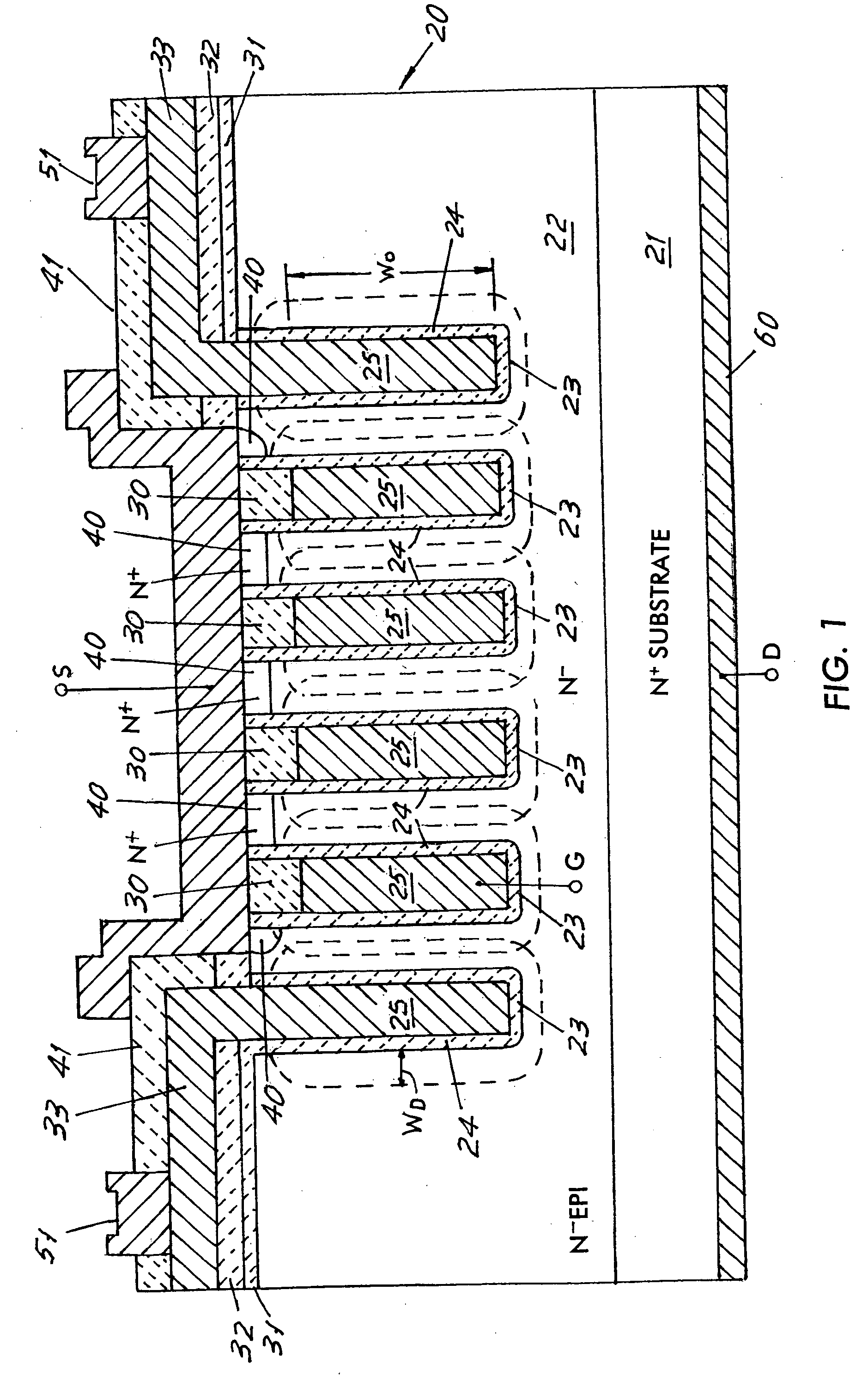
[0017]FIG. 1 is a cross-section of a small section of a FET die constructed in accordance with the invention.

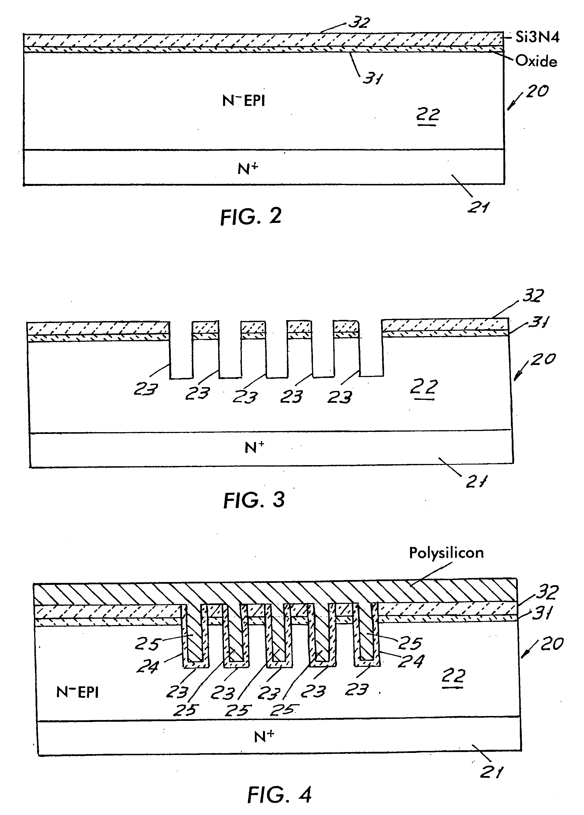
[0018]FIG. 2 is a cross-section of the starting wafer for making the device of FIG. 1 after initial oxidation and nitride deposition steps.

[0019]FIG. 3 shows the wafer of FIG. 2 after a trench mask step and the formation of a plurality of trenches into its top surface.

[0020]FIG. 4 shows the wafer of FIG. 3 after gate oxidation and polysilicon deposition steps.

[0021]FIG. 5 shows the wafer of FIG. 4 after a polysilicon mask step and polysilicon etch-back and oxidation.

[0022]FIG. 6 shows the wafer of FIG. 6 after TEOS deposition, a contact mask step and a TEOS etch and resist stip.

[0023]FIG. 7 shows the wafer of FIG. 6 after a nitride etch and an N+ implant and anneal step.

[0024]FIG. 8 shows the wafer of FIG. 7 after a metal deposition and sputter step, and metal patterning, forming the device of FIG. 1.

[0025]FIG. 9 shows an embodiment of the invention in which each of t...


PUM


Abstract

A vertical conduction trench FET has a plurality of trenches containing conductive polysilicon gates. The mesas between the trenches have a source diffusion region connected to a common source electrode. The trenches are spaced so that the depletion regions induced by the trench gate will overlap to pinch off conduction through the mesa to turn off the device. The gate potential is pulsed. The polysilicon in the trenches may be separated into two insulated portions. The pulses may be applied simultaneously or sequentially to the polysilicon gates.

Description

RELATED APPLICATIONS [0001] This application claims the benefit and priority of U.S. Provisional Application No. 60 / 587,745, filed Jul. 14, 2004, the entire disclosure of which is incorporated by reference herein.FIELD OF THE INVENTION [0002] This invention relates to field effect transistors (FETs) and more specifically to a trench type FET in which the mesas between the trenches are dynamically depleted by gate structures to turn off the device. BACKGROUND OF THE INVENTION [0003] Enhancement trench type power MOSFETs are well known. Such devices employ a conventional base or channel region which is inverted by gate potential applied to polysilicon gates buried in the trenches and insulated from the trench walls by a gate oxide or other oxide layers. [0004] In the Depletion Trench MOSFET it is the accumulation region (as opposed to inversion region) that provides the device conduction as well as the bulk of the mesa. [0005] The impurity concentration of the mesa regions and the bod...

Claims


Application Information

Patent Timeline
IPC IPC(8): H01L29/76
CPCH01L29/66666H01L29/7828H01L29/7827
Inventor BOL, IGORLI, XIN
Owner INFINEON TECH AMERICAS CORP
Why Eureka
Try Eureka