Supercharge Your Innovation With Domain-Expert AI Agents!

High speed integrated circuit

a high-speed integrated circuit and circuit technology, applied in logic circuits, logic circuit coupling/interface arrangements, pulse techniques, etc., can solve the problems of affecting the performance of output interfaces, differential interface designs have disadvantages, and the majority of previously disclosed driver circuits are not suitable for high-speed signals. performance improvement

Inactive Publication Date: 2006-01-26
KAO RICHARD F C
View PDF24 Cites 25 Cited by
  • Summary
  • Abstract
  • Description
  • Claims
  • Application Information

AI Technical Summary

Benefits of technology

[0006] An embodiment of the invention is a single-ended output interface that uses a differential driver as a design backbone. Unlike a conventional differential interface, which typically has two or more outputs for providing an output signal and its complement, the differential driver of the present embodiment has one of its outputs coupled to drive a signal onto a signal line, while a complementary output is not used for signal transmission. Rather, the complementary output is considered logically redundant and is terminated, for example, by coupling to package ground or system ground via a capacitor. A result of terminating a logically redundant output is that the performance of the output interface may be significantly improved over conventional designs.
[0007] In one embodiment of the invention, multiple differential drivers are implemented within an integrated circuit that has a package ground plane. According to this embodiment, each “unused” output of the differential drivers may be terminated at the package ground plane through a capacitor. The package ground plane itself may be coupled to one or more GND pins. In this way, very few pins are needed by the “unused” outputs. Furthermore, only one signal line is needed for each single-ended output signal. In comparison to conventional differential interfaces, where two pins and two signal lines are required for each differential signal, the number of pins and signal lines used by the present embodiment may be significantly smaller.
[0008] Another embodiment of the invention is an integrated circuit having a single-ended input and multiple single-ended outputs, for instance a clock driver. Within the integrated circuit, the input signal is first converted into a differential signal. The differential signal is distributed to the multiple differential drivers. Each differential driver may have an output for providing a single-ended output signal and an “unused” output, which terminates one component of the differential signal. Each “unused” output may be coupled to package ground or system ground via a capacitor for the purpose of improving the performance of the other output.
[0009] Another embodiment of the invention is an integrated circuit having single-ended inputs and single-ended outputs. The single-ended outputs are implemented using differential drivers each having one output that is “unused.” Within the integrated circuit, differential signals may be originated, processed and distributed to the multiple differential output driver circuits. Each differential driver may have an output for providing a single-ended output signal and an “unused” output. The “unused” output of each differential driver may be coupled to package ground or system ground via a capacitor for the purpose of improving the performance of the other output. Circuits that process differential signals within the integrated circuits may be implemented with differential standard cells in accordance with some embodiments of the invention.

Problems solved by technology

However, most of these previously disclosed driver circuits are not suitable for high speed signals due to their low maximum operating frequency and high noise.
However, differential interface designs have disadvantages as well.
This design requirement is sometimes known as “length matching” or “delay matching.” A wide differential interface will require a large number of signal lines, necessarily complicating the length matching effort and increasing the cost of manufacture.
In some instances, length matching many signal lines may be impossible on tightly packed circuit boards.
Thus, at least in some electronic systems, it is not desirable to use differential interfaces.

Method used


Image

  • High speed integrated circuit
  • High speed integrated circuit
  • High speed integrated circuit

Examples


Embodiment Construction

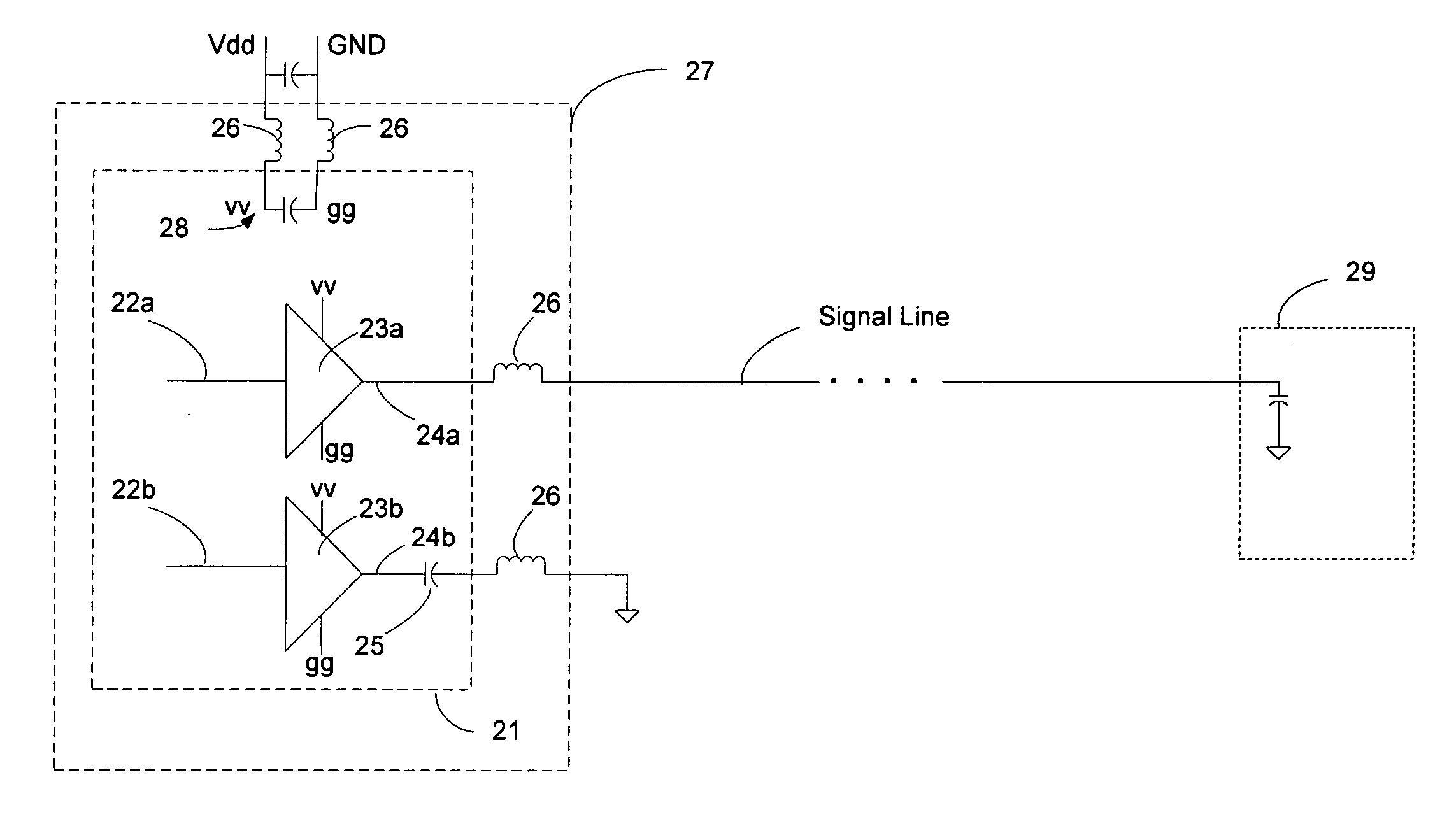
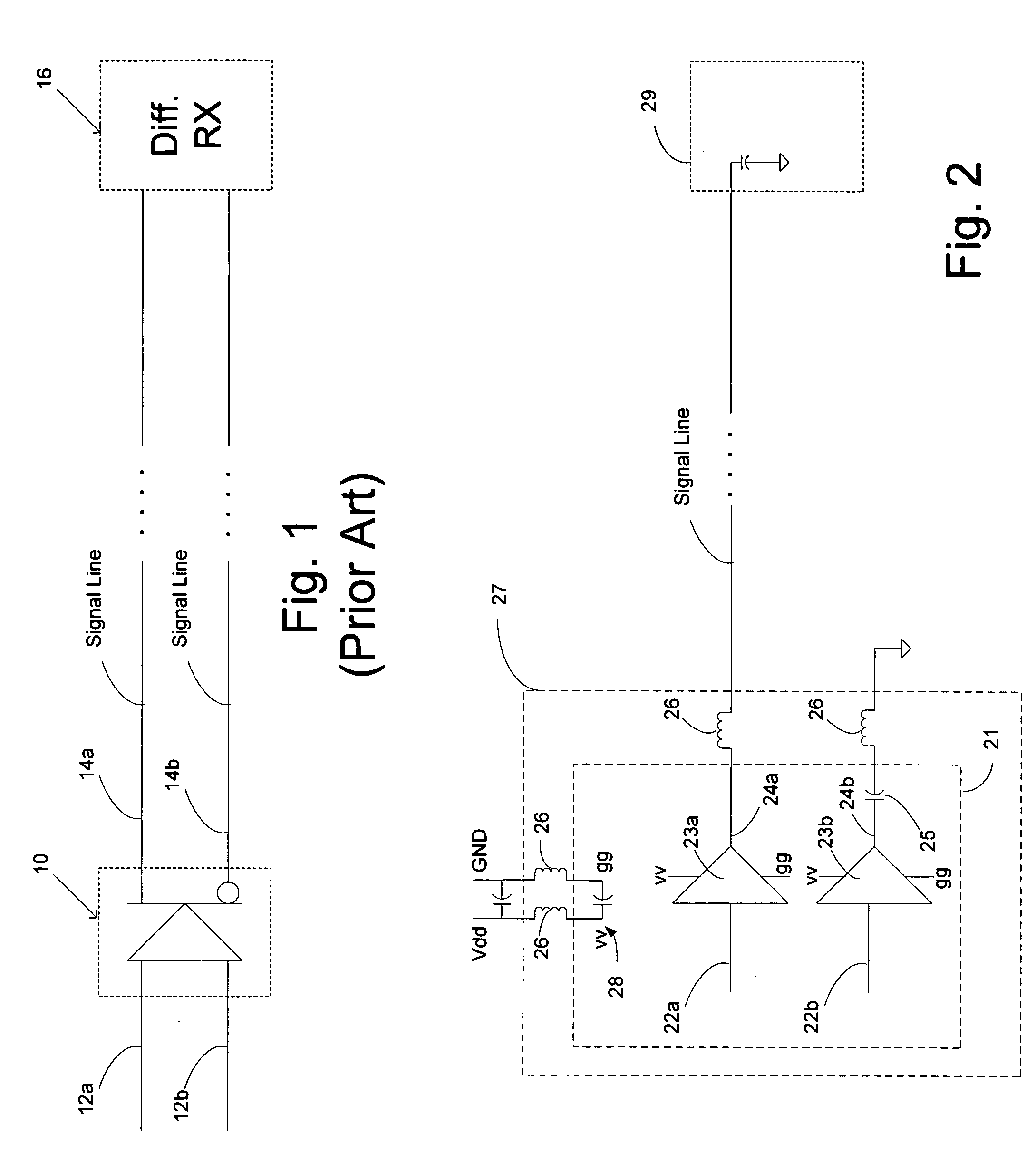
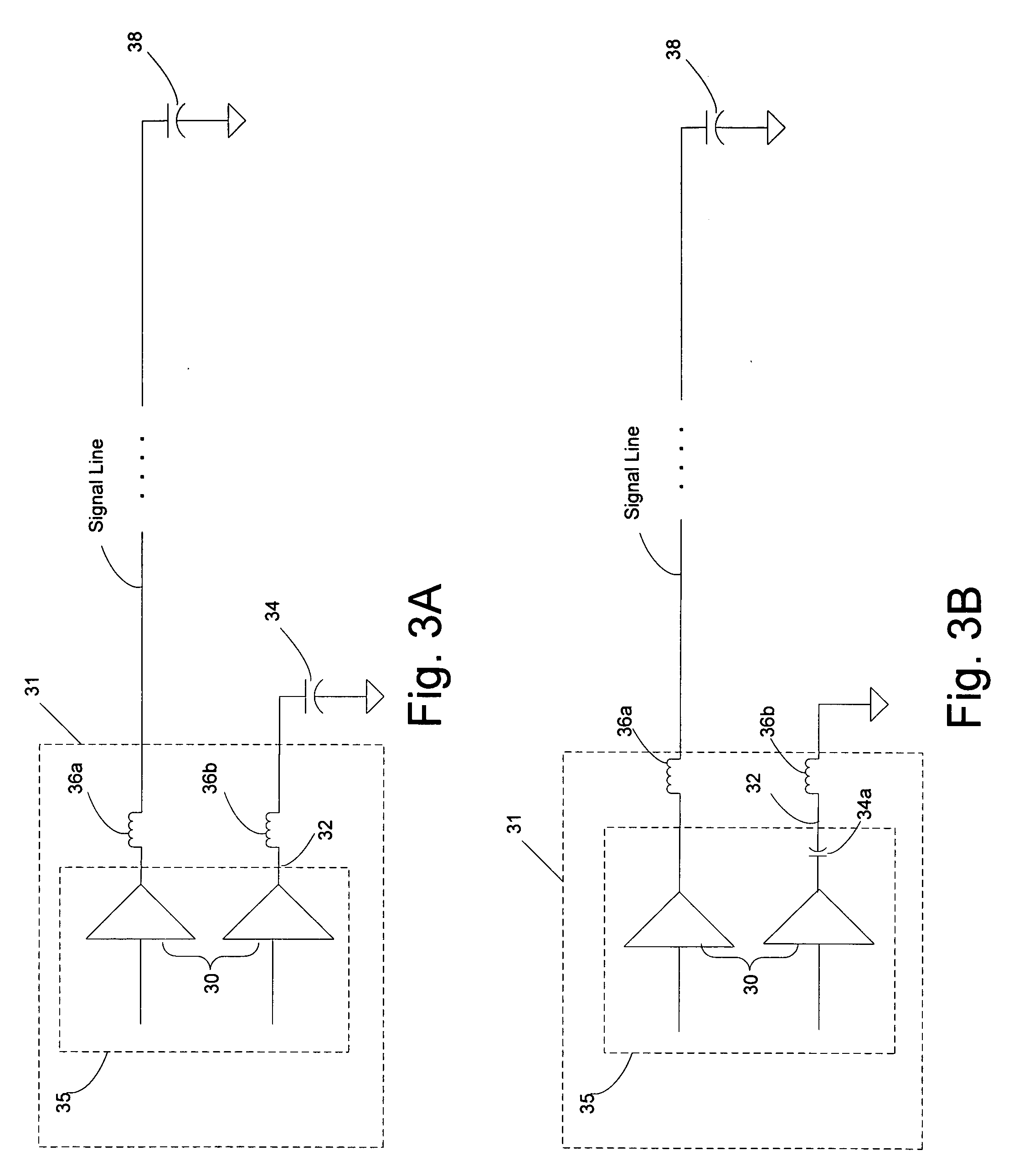
[0032] Various features of the invention, including specific implementations thereof; will now be described. Throughout the description, the term “differential signal” refers to a signal that is carried by more than one signal lines, and thus a differential signal includes two or more component signals that may be complementary to each other. If the sum of two time-varying signals always approximately equals a constant value, such as zero, the signals are said to be “complementary” to each other. The term “single-ended signal” refers to a signal that is carried by a single signal line. Furthermore, the terms “driver” and “driver circuit” are used synonymously.

[0033] Throughout the description, the term “unused output” refers to an output of a differential output driver that is not used to provide a signal to a receiver, or one that is not used to drive a signal line. The term “unused output” may also refer to an output of a differential output driver that may be coupled to package ...


PUM


Abstract

A novel driver circuit that uses a differential driver as a design backbone is described. Unlike a conventional differential interface, which typically has two or more outputs for providing an output signal and its complement, one of the differential driver's outputs is coupled to drive an output signal onto a signal line, while another one of the differential driver's outputs is unused and terminated, for instance by coupling the output to package ground or a voltage source via a capacitor. The performance of the driver circuit is significantly improved over conventional singled-ended driver designs.

Description

FIELD OF THE INVENTION [0001] The present invention relates generally to digital communication interface and more specifically to high speed circuit designs. BACKGROUND OF THE INVENTION [0002] A signal line is a conductor used to transmit electrical signals between various devices in an electronic system or between devices located in two separate electronic systems. Output driver circuits contained on each device are used to buffer signals originating from the device so that they may be driven onto the signal lines. [0003] There are well known single-ended output driver circuits (e.g., TTL drivers) that are simple to use. However, most of these previously disclosed driver circuits are not suitable for high speed signals due to their low maximum operating frequency and high noise. For example, the maximum operating frequency of a single-ended CMOS driver circuit IDT74FCT3807D / E, which is available from Integrated Device Technology, Inc. of Santa Clara, Calif., is 166 Mhz. [0004] For ...

Claims


Application Information

Patent Timeline
Patent Type & Authority Applications(United States)
IPC IPC(8): H03K19/0175
CPCH03K19/0948H03K19/018578H01L2224/05554H01L2224/48247H01L2224/48257H01L2224/49171H01L2924/19107
Inventor KAO, RICHARD F. C.
Owner KAO RICHARD F C
Features
  • R&D
  • Intellectual Property
  • Life Sciences
  • Materials
  • Tech Scout
  • Unparalleled Data Quality
  • Higher Quality Content
  • 60% Fewer Hallucinations
Learn More