Clocked inverter, NAND, NOR and shift register

a technology of shift register and clock inverter, which is applied in the direction of generating/distributing signals, pulse techniques, instruments, etc., can solve the problems of increasing the total size of the device casing, reducing the frequency property, and increasing the occupation area of the driver circuit, so as to reduce the area occupied by the driver circuit, the effect of reducing manufacturing costs and power consumption

Inactive Publication Date: 2008-02-05
SEMICON ENERGY LAB CO LTD
View PDF29 Cites 33 Cited by
  • Summary
  • Abstract
  • Description
  • Claims
  • Application Information

AI Technical Summary

Benefits of technology

[0009]The present invention has been made in view of the above problems. It is an object of the present invention to realize miniaturization of a casing for devices and to reduce manufacturing costs and power consumption by providing the shift register without arranging any level shifter in an external circuit. Further, according the present invention, the shift register can be achieved without arranging any level shifter in an internal circuit to solve such problems that the waveform of CK is delayed and blunted and that the voltage of a power source line arranged in the internal circuit is dropped. Also, the reduction of an area occupied by a driver circuit in the internal circuit, the reduction of power consumption, and a high frequency operation can be realized.
[0010]Further, it is another object of the present invention to provide a clocked inverter, a shift register that can be operated accurately by mitigation of the influence of the fluctuation in the property of TFT. Moreover, it is possible to provide a NAND circuit or a NOR circuit that has lower input load and higher output ability as compared to conventional NAND circuit or NOR circuit.
[0049]Also, no level shifter is arranged in an external circuit, so that the miniaturization of a casing, the reduction of manufacturing costs, and the reduction of power consumption are realized. Further, the shift register is achieved without arranging any level shifter in an internal circuit. As a result, such problems that the waveform of CK is delayed and blunted and that the voltage of a power source line arranged in the internal circuit is dropped are solved. Also, the reduction of an area occupied by a driver circuit in the internal circuit, the reduction of power consumption, and a high frequency operation are realized.

Problems solved by technology

When level shifting is performed in an internal circuit, problems are caused, for example, in increase in occupation area of a driver circuit, reduction of frequency property due to delayed or blunted waveforms.
On the contrary, when a level shifter is arranged in an external circuit, problems are caused, for example, growth in total size of a casing for devices due to the increase in the number of components such as IC, in cost for manufacturing and in power consumption by the shift register.

Method used


Image

  • Clocked inverter, NAND, NOR and shift register
  • Clocked inverter, NAND, NOR and shift register
  • Clocked inverter, NAND, NOR and shift register

Examples


embodiment mode 1

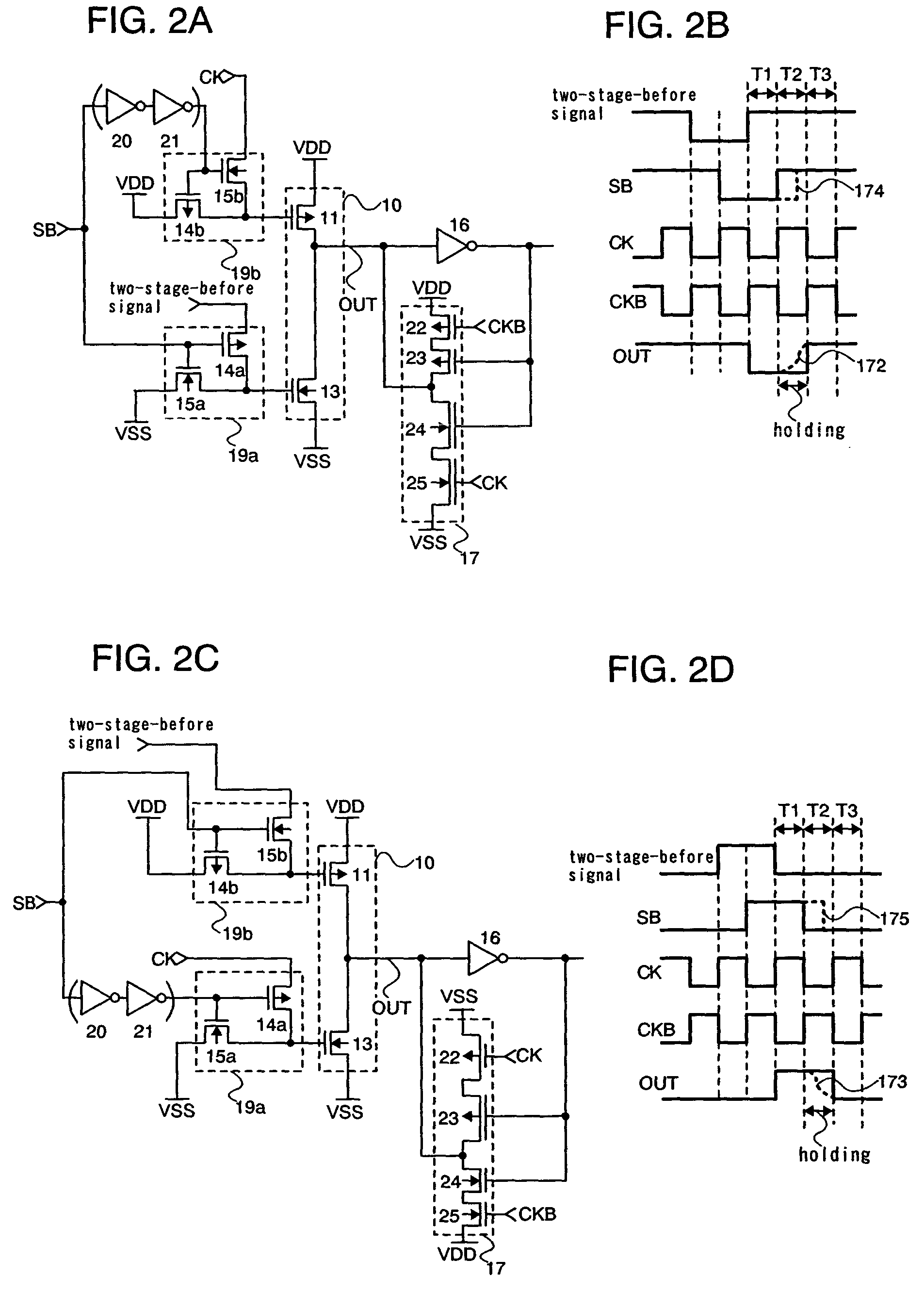
[0064]This embodiment mode of the present invention will be described below with reference to FIGS. 1A to 1D. In this embodiment mode, as an example, it is assumed that CK is switched between 5 V (H level) and 2 V (L level), VDD (high potential power source) is 7 V, and VSS (low potential power source) is 0 V. That is, it is assumed that the amplitude of CK is 3 V and a power source voltage amplitude is 7 V.

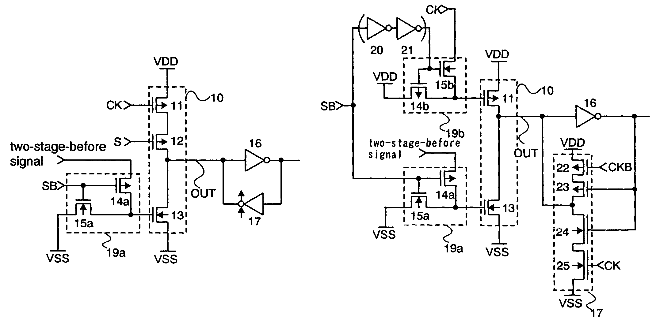
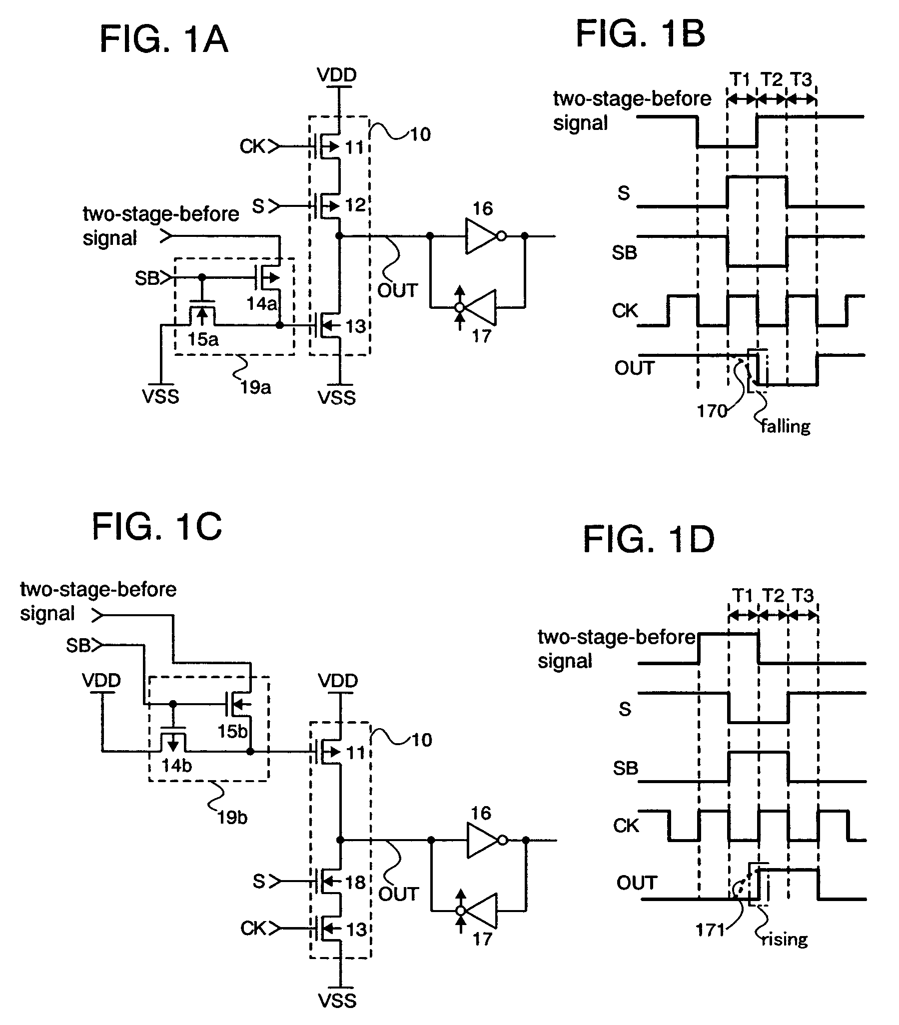
[0065]A first structure of the present invention will be described with reference to FIG. 1A. FIG. 1A is a circuit diagram showing structural elements of a shift register arranged in the n-th stage. Each stage is formed by a clocked inverter 10 including TFTs 11 to 13 connected in series, a compensation circuit 19a including TFTs 14a and 15a connected in series, an inverter 16, and a clocked inverter 17. The shift register is formed by cascade-connecting the respective stages, in which these circuits are arranged, with signals from CK and CKB being alternately inputted at the res...

embodiment mode 2

[0133]It is possible to use the first to sixth structures described above with reference to FIGS. 1A to 1D, 2A to 2D, and 3A to 3D by freely combining them. In this embodiment mode, an example of the combination will be described with reference to FIGS. 6A and 6B and FIGS. 7A and 7B. Note that in those drawings, a signal S is a start pulse or an output of a clocked inverter 16 arranged at the (n−1)th stage, and a signal SB corresponds to the inverted signal of the signal S. Also, the term “two-stage-before signal” corresponds to the output of the clocked inverter 10 arranged at the (n−2)th stage.

[0134]FIG. 6A is a circuit diagram in which the third structure (see FIG. 2A) and the fifth structure (see FIG. 3A) are combined, and shows structural elements of a shift register arranged at the n-th stage. Each stage is formed by a clocked inverter 10 including TFTs 71 to 73 connected in series, an inverter 16, a clocked inverter 17 including TFTs 74 and 75 connected in series, TFTs 76 and...

embodiment mode 3

[0139]This embodiment mode according to the present invention will be described with reference to FIGS. 10A and 10B.

[0140]FIG. 10A shows a plan layout view (top view) of the circuit diagram shown in FIG. 6B. FIG. 10B shows a photograph of a panel that is actually made, magnified by a light microscope.

[0141]Reference numerals and symbols in FIGS. 10A and 10B correspond to those in FIG. 6B, and thus the description is omitted here. In FIGS. 10A and 10B, a P-type TFT 16a and an N-type TFT 16b constitute an inverter 16, and a P-type TFT 123a and an N-type TFT 123b constitute an analog switch 123.

[0142]The W (gate width) of the TFT 94 is set large. If another TFT that is connected with the TFT 94 in series and has the same size as the TFT 94 is required, the layout area becomes larger. However, only one TFT 94 whose W is set large is required in the present invention, and therefore the expansion of the layout area is suppressed.


PUM


Abstract

A threshold voltage of a transistor is fluctuated because of fluctuation in film thickness of a gate insulating film or in gate length and gate width caused by differences of used substrates or manufacturing steps. In order to solve the problem, according to the present invention, there is provided a clocked inverter including a first transistor and a second transistor connected in series, and a compensation circuit including a third transistor and a fourth transistor connected in series. In the clocked inverter, gates of the third transistor and the fourth transistor are connected to each other, drains of the third transistor and the fourth transistor are each connected to a gate of the first transistor, sources of the first transistor and the fourth transistor are each electrically connected to a first power source, a source of the second transistor is electrically connected to a second power source, and an amplitude of a signal inputted to a source of the third transistor is smaller than a potential difference between the first power source and the second power source.

Description

BACKGROUND OF THE INVENTION[0001]1. Field of the Invention[0002]The present invention relates to a clocked inverter and also relates to a shift register including a clocked inverter as a unit circuit. Further, the present invention relates to electric circuits such as a NAND and a NOR.[0003]2. Description of the Related Arts[0004]In recent years, display devices such as a liquid crystal display device and a light emitting device have been developing greatly because of the growth in demand of mobile machines. A technique for integrating a pixel and a driver circuit (hereinafter, internal circuit) using a transistor formed of a polysilicon semiconductor on an insulator has been developing greatly, because the technique can contribute to miniaturization of devices and less electric power consumption. The internal circuit formed on an insulator is connected with a controller IC or the like (hereinafter, external circuit) thorough a FPC or the like to be controlled.[0005]Generally, the p...

Claims


Application Information

Patent Timeline
Patent Type & Authority Patents(United States)
IPC IPC(8): H03K19/20G09G3/20G11C19/00G11C19/28H03K19/003H03K19/096
CPCG11C19/00G11C19/28H03K19/0963H03K19/018521H03K19/00384G09G3/20
Inventor OSAME, MITSUAKIANZAI, AYA
Owner SEMICON ENERGY LAB CO LTD
Why Eureka
Try Eureka