Shift register, display device, and electronic device

a shift register and display device technology, applied in the field of shift registers, can solve the problems of increasing reducing the frequency property, and increasing the total size of the device casing, so as to achieve the effect of reducing the occupation area of the shift register over the substra

Active Publication Date: 2006-10-19
SEMICON ENERGY LAB CO LTD
View PDF47 Cites 19 Cited by
  • Summary
  • Abstract
  • Description
  • Claims
  • Application Information

AI Technical Summary

Benefits of technology

[0014] By implementing the present invention, a shift register which can operate without providing a particular level shift portion can be provided, the occupation area of a shift register over a substrate can be reduced. By implementing the present invention, a shift register can be provided, which can turn OFF a p-channel transistor included in the other clocked inverter by using a potential of a high potential power source output via one of two clocked inverters provided in the register. In addition, a shift register of the present invention can turn OFF an n-channel transistor by each setting a potential on Low Level of the clock signal and a potential of a low potential power source equal in a case that a clock signal having a smaller amplitude than a potential difference between a high potential power source and a low potential power source is input. By turning OFF a transistor in this manner, an unintended through current in each transistor can be reduced. By implementing the present invention, a potential of a low potential power source which is output via one of two clocked inverters provided in a register is used to turn OFF an n-channel transistor included in the other clocked inverter. In addition, a shift register of the present invention can turn OFF a p-channel transistor by setting a potential on High Level of the clock signal and a potential of a high potential power source equal in a case that a clock signal having a smaller amplitude than a potential difference between a high potential power source and a low potential power source is input. By turning OFF a transistor in this manner, an unintended through current in each transistor can be reduced.

Problems solved by technology

When level shifting is performed in an internal circuit, problems are caused, for example, in increase in occupation area of a driver circuit, reduction of frequency property due to delayed or blunted waveforms.
On the contrary, when a level shifter is arranged in an external circuit, problems are caused, for example, growth in total size of a casing for devices due to the increase in the number of components such as IC, in cost for manufacturing and in power consumption by the shift register.

Method used


Image

  • Shift register, display device, and electronic device
  • Shift register, display device, and electronic device
  • Shift register, display device, and electronic device

Examples


embodiment mode 1

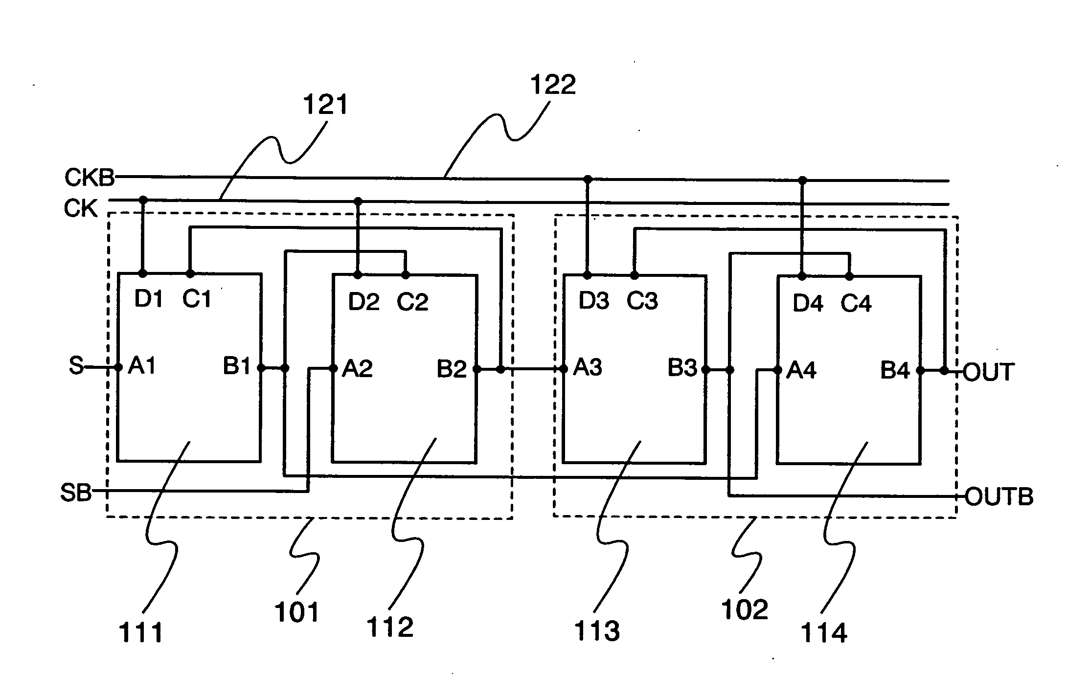
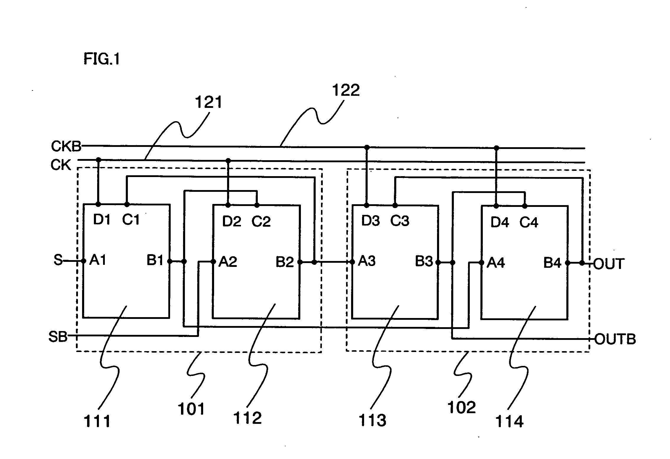
[0024]FIG. 1 is a circuit diagram showing one mode of a shift register of the present invention. In FIG. 1, a register 101 of a (2n−1)-th stage (n is an arbitrary integer number, m is the total number of stages provided in a shift register, m≧2n≧n) and a register 102 of a 2n-th stage are shown. The register 101 includes a first clocked inverter 111 and a second clocked inverter 112, and the register 102 includes a first clocked inverter 113 and a second clocked inverter 114. These clocked inverters are each connected to a high potential power source VDD and a low potential power source VSS.

[0025] The first clocked inverter 111 has an input terminal A1, an output terminal B1, an input terminal C1, and an input terminal D1; the second clocked inverter 112 has an input terminal A2, an output terminal B2, an input terminal C2, and an input terminal D2; the first clocked inverter 113 has an input terminal A3, an output terminal B3, an input terminal C3, and an input terminal D3, and the...

embodiment mode 2

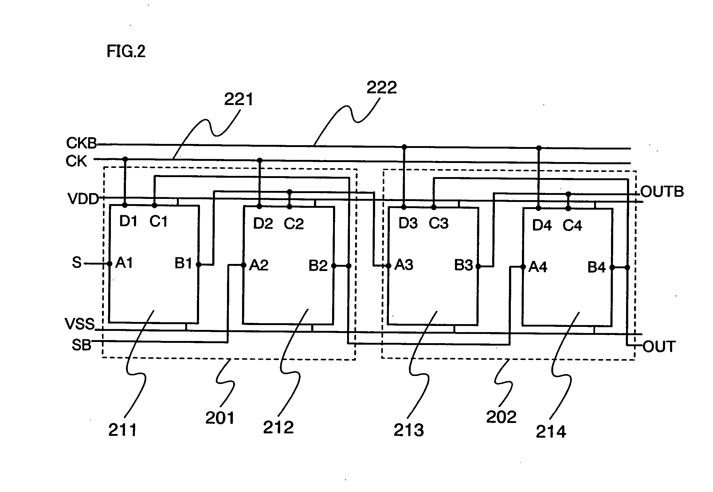
[0037]FIG. 2 shows a circuit diagram showing one mode of a shift register of the present invention. The circuit diagram of FIG. 2 is different from that of FIG. 1 in the connection of input terminals A1, A2, A3, A4 and output terminals B1, B2, B3, B4. In FIG. 2, a register 201 at a (2n−1)-th stage (n is an arbitrary integer number, m is the total number of stages provided in a shift register, m≧2n≧n) and a register 202 at a 2n-th stage are shown. The register 201 includes a first clocked inverter 211 and a second clocked inverter 212, and the register 202 includes a first clocked inverter 213 and a second clocked inverter 214. These clocked inverters are each connected to a high potential power source VDD and a low potential power source VSS.

[0038] The first clocked inverter 211 has an input terminal A1, an output terminal B1, an input terminal C1, and an input terminal D1; the second clocked inverter 212 has an input terminal A2, an output terminal B2, an input terminal C2, and an...

embodiment mode 3

[0050] In Embodiment Mode 3, a concrete structure of each register included in the shift register described in Embodiment Mode 1 is described with reference to FIGS. 5A and 5B, exemplifying a structure of a clocked inverter. There is no particular limitation on a first clock signal, a high potential power source VDD, and a low potential power source VSS; however, for clear description, a signal at High Level of the first clock signal is e.g., 3V and a signal at Low Level is e.g., 0 V here. In addition, the high potential power source (VDD) is e.g., 7V and the low potential power source (VSS) is e.g., 0 V. In FIGS. 5A and 5B, a first clocked inverter 50 surrounded by a dotted line corresponds to the first clocked inverter 111 of Embodiment Mode 1, and a second clocked inverter 60 surrounded by a dotted line corresponds to the second clocked inverter 112 of Embodiment Mode 1.

[0051] The first clocked inverter 50 includes transistors 51 to 54 which are connected in series, and the seco...


PUM


Abstract

The present invention provides a shift register which can operate favorably without providing a level shift portion. The first clocked inverter at the (2n−1)-th stage operates in accordance with the first output from the previous stage, an output from the second clocked inverter at the previous stage, and the first CK signal; the second clocked inverter at the (2n−1)-th stage operates in accordance with the second output from the previous stage, an output of the first clocked inverter at the (2n−1)-th stage, and the first CK signal; one of the first output and the second output is equal to a potential of VDD and the other is equal to a potential of VSS; the first CK signal at the 2n-th stage operates the third output from the (2n−1)-th stage, an output of the second clocked inverter and the second CK signal; the second clocked inverter at the 2n-th stage operates in accordance with the fourth output from the (2n−1)-th stage, an output from the first clocked inverter at the 2n-th stage, and the second CK signal; one of the third output and the fourth output is equal to the potential of VDD and the other is equal to the potential of VSS, and the second CK signal is an inversion signal of the first CK signal and the amplitude of the CK signal is smaller than the power supply potential.

Description

FIELD OF THE INVENTION [0001] The present invention relates to a shift register which each includes a clocked inverter as unit circuit. BACKGROUND ART [0002] In recent years, display devices such as a liquid crystal display device or a light-emitting device have been developed actively because of the growth in demand for portable devices. In particular, an integration technique in which a pixel and a driver circuit (hereinafter, referred to as an internal circuit) using a transistor formed from a polycrystalline semiconductor over an insulator, has been developed actively, since the technique greatly contributes to miniaturization and lower power consumption. An internal circuit formed over the insulator is connected to a controller IC (hereinafter, referred to as an external circuit) or the like via FPC or the like and the operation is controlled. [0003] A power supply potential of an internal circuit is usually around 10V, while an IC constituting an external circuit prepares a si...

Claims


Application Information

Patent Timeline
Patent Type & Authority Applications(United States)
IPC IPC(8): G11C19/00
CPCG09G3/3674G11C19/28G11C19/00G09G3/3685
Inventor OSAME, MITSUAKIANZAI, AYASATO, MIZUKI
Owner SEMICON ENERGY LAB CO LTD
Why Eureka
Try Eureka