Supercharge Your Innovation With Domain-Expert AI Agents!

Semiconductor constructions

a technology of semiconductors and constructions, applied in the direction of transistors, ear rings, solid-state devices, etc., can solve the problems of increasing junction leakage in source/drain regions, reducing the threshold voltage of a device, and increasing the junction leakage in the source/drain region

Inactive Publication Date: 2006-01-26
MICRON TECH INC
View PDF99 Cites 1 Cited by
  • Summary
  • Abstract
  • Description
  • Claims
  • Application Information

AI Technical Summary

Benefits of technology

The invention is about a semiconductor construction with two channel regions that have a sub-region doped with indium or heavy atom acceptor atoms. The channel also contains boron surrounding the sub-region. A pair of transistor constructions is disposed over the semiconductor substrate, each constructed over one of the channel regions. The transistor constructions are separated by an isolation region. Each transistor construction has a transistor gate that is wider than the underlying indium doped sub-region. The invention also includes methods of forming semiconductor constructions. The technical effect of the invention is to provide a semiconductor construction with improved performance and reliability.

Problems solved by technology

However, a threshold voltage of a device reduces with the decrease in gate oxide thickness.
Increasing dopant levels in channels of the devices can increase the threshold voltage to an acceptable level and compensate for the reduction in gate oxide thickness, but can increase junction leakage in source / drain regions.
Additionally, the increased dopant level in a channel of a device can adversely cause junction capacitance to increase, cause channel mobility reduction, and reduce the current drive of the device.

Method used


Image

  • Semiconductor constructions
  • Semiconductor constructions
  • Semiconductor constructions

Examples


Embodiment Construction

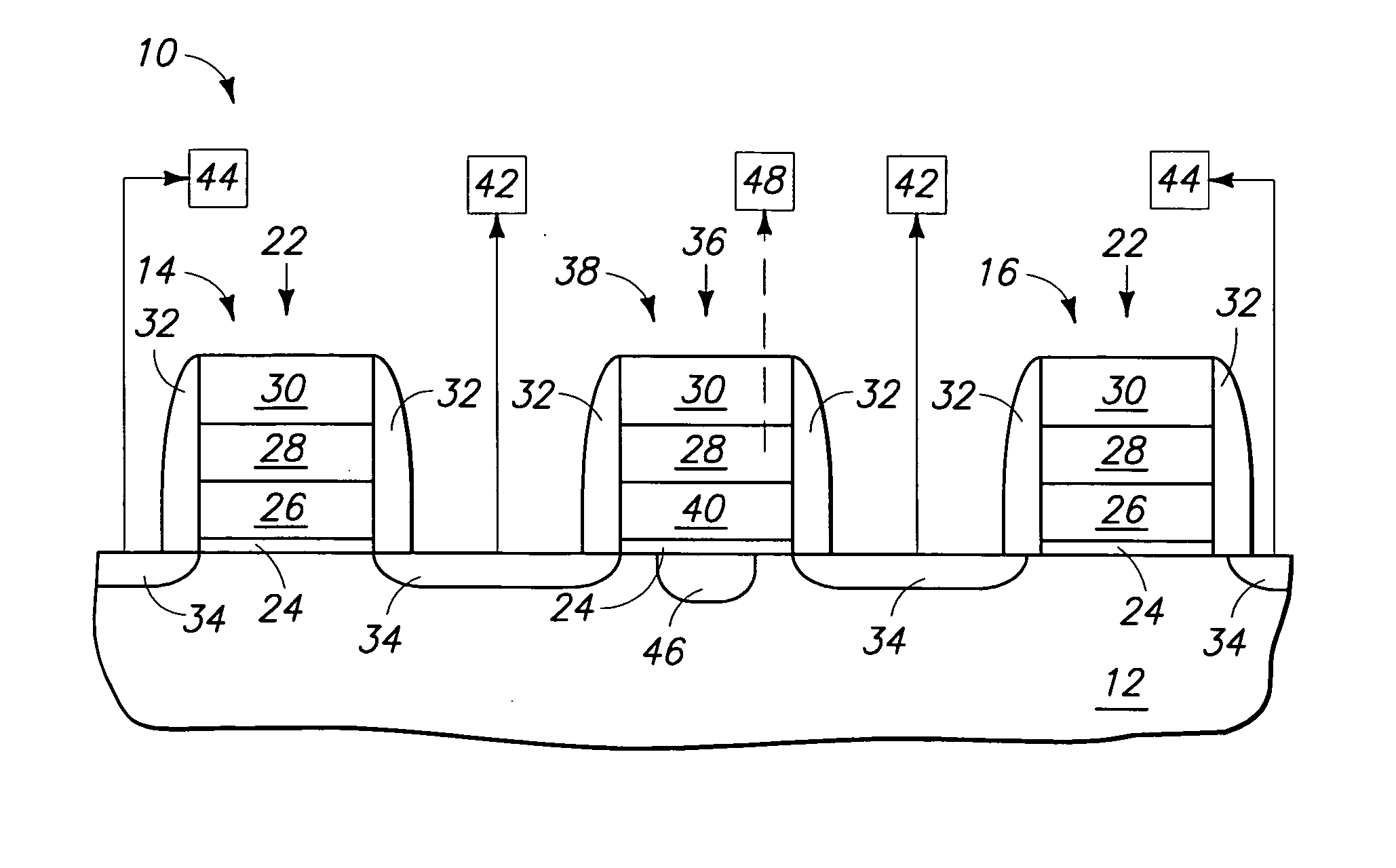
[0038]FIG. 1 illustrates a semiconductor construction 10 encompassed by particular aspects of the present invention. Construction 10 comprises a substrate 12. To aid in interpretation of the claims that follow, the terms “semiconductive substrate” and “semiconductor substrate” are defined to mean any construction comprising semiconductive material, including, but not limited to, bulk semiconductive materials such as a semiconductive wafer (either alone or in assemblies comprising other materials thereon), and semiconductive material layers (either alone or in assemblies comprising other materials). The term “substrate” refers to any supporting structure, including, but not limited to, the semiconductive substrates described above.

[0039] In particular aspects, construction 10 can correspond to a DRAM array. Construction 10 comprises a pair of field effect transistor devices 14 and 16 supported by substrate 12, and also comprises a device 38 having a different threshold voltage than ...


PUM


Abstract

The invention includes a semiconductor construction having a pair of channel regions that have sub-regions doped with indium and surrounded by boron. A pair of transistor constructions are located over the channel regions and are separated by an isolation region. The transistors have gates that are wider than the underlying sub-regions. The invention also includes a semiconductor construction that has transistor constructions with insulative spacers along-gate sidewalls. Each transistor construction is between a pair source / drain regions that extend beneath the spacers. A source / drain extension extends the source / drain region farther beneath the transistor constructions on only one side of each of the transistor constructions. The invention also includes methods of forming semiconductor constructions.

Description

TECHNICAL FIELD [0001] The invention pertains to semiconductor constructions and methods of forming semiconductor constructions. In particular aspects, the invention pertains to methods of forming DRAM constructions. BACKGROUND OF THE INVENTION [0002] Electrical isolation is commonly utilized in semiconductor constructions to alleviate, or prevent, leakage between electrical devices. For instance, it is frequently desired in dynamic random access memory (DRAM) fabrication to avoid sub-threshold leakage between access devices (such as, for example, access transistor constructions). There can be several facets which influence leakage currents between field effect transistor devices, including, for example, junction leakage in source / drain regions; drain-induced barrier lowering (DIBL) due to short gate lengths; gate-induced drain leakage (GIDL) due to high electric fields in a gate overlap region; narrow-width effects; and stress-induced leakage current (SILC) due to a proximity of an...

Claims


Application Information

Patent Timeline
Patent Type & Authority Applications(United States)
IPC IPC(8): H01L21/8238H01L21/76H01L29/00H01L27/08H10B10/00A44C7/00H01L21/00H01L21/28H01L21/3205H01L21/336H01L21/4763H01L21/82H01L21/8234H01L21/84H01L27/088H01L27/10H01L29/10H01L29/49H01L29/78H01L31/062H01L31/113H10B12/00
CPCH01L21/28044Y10S438/919H01L21/823418H01L21/823425H01L27/10873H01L27/10888H01L27/10891H01L27/10894H01L29/1041H01L29/4916H01L29/66537H01L29/66553H01L29/66583H01L29/6659H01L29/78Y10S438/975H01L21/823412H10B12/05H10B12/488H10B12/485H10B12/09H01L21/18
Inventor TRAN, LUAN C.
Owner MICRON TECH INC
Features
  • R&D
  • Intellectual Property
  • Life Sciences
  • Materials
  • Tech Scout
  • Unparalleled Data Quality
  • Higher Quality Content
  • 60% Fewer Hallucinations
Learn More