Termination circuit

Active Publication Date: 2006-02-02
FUJITSU LTD
View PDF5 Cites 10 Cited by
  • Summary
  • Abstract
  • Description
  • Claims
  • Application Information

AI Technical Summary

Benefits of technology

[0033] As described above, according to the present invention, the matching characterist

Problems solved by technology

However, it is often difficult in connection with other circuits to unify a plurality of wiring layouts to the gate terminal of each transistor.
Therefore, in the technology disclosed in the Japanese Patent Application No. 2002-344300, voltage

Method used


Image

  • Termination circuit
  • Termination circuit
  • Termination circuit

Examples


Embodiment Construction

[0039] The preferred embodiments of the present invention are described below with reference to the drawings.

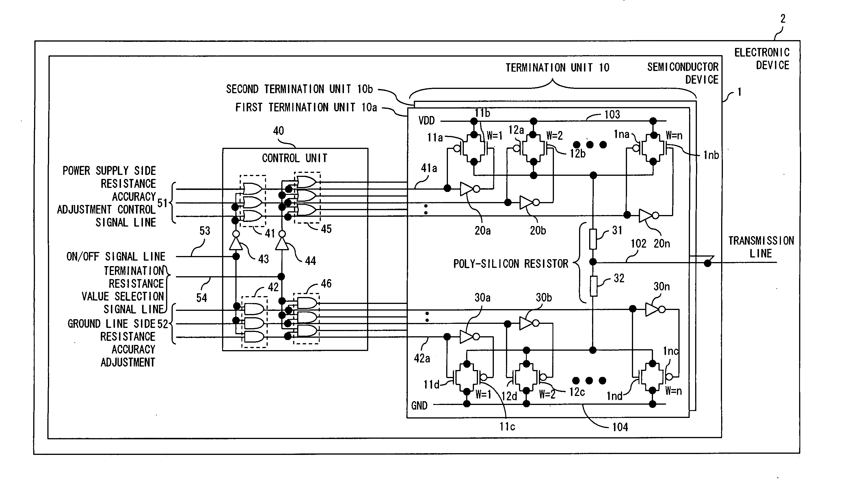
[0040]FIG. 3 shows the configuration of the termination circuit for implementing the present invention. In FIG. 3, the same reference numerals are attached to the same lines as in FIG. 2.

[0041] In this preferred embodiment, this termination circuit is formed on a single semiconductor substrate in a semiconductor device 1. This semiconductor device 1 is, for example, a central processing unit (CPU), and is provided for an electronic device 2, such as a computer or the like.

[0042] The termination circuit shown in FIG. 3 comprises a termination unit 10 for forming Thevenin termination and a control unit 40 for controlling both the switching of activation / inactivation of the terminal circuit and switching of a termination resistance value.

[0043] The termination unit 10 comprises both a first termination unit 10a and a second termination unit 10b for each transmission line 102...


PUM


Abstract

A termination circuit for terminating a transmission line comprises a resistance unit which is formed by connecting a P-channel type MOS transistor and an N-channel type MOS transistor in parallel, and Thevenin termination is formed by providing this resistance unit between the transmission line and a power supply line and between the transmission line and a ground line.

Description

BACKGROUND OF THE INVENTION [0001] 1. Field of the Invention [0002] The present invention relates to a signal transmission technology, more particularly to a technology for a termination circuit for matching a plurality of segments of impedance of a transmission line. [0003] 2. Description of the Related Art [0004] In a memory interface based on double data rate 2 (DDR2) rating stipulated by Joint Electron Device Engineering Council (JEDEC), it is required that a termination circuit should be provided on the controller side of memory. [0005] It is required that the termination circuit on the controller side in a DDR2 interface is activated when a controller receives data, and it is inactivated when the controller transmits data. It is stipulated that the matched impedance of a transmission line should be 75 ohms. Therefore, if a controller and memory are connected 1 to 1, the termination resistance value is made to be 75 ohms. However, if a controller and memory are connected 1 to 2...

Claims


Application Information

Patent Timeline
IPC IPC(8): H03K19/003
CPCH04L25/0298H03K19/0005
Inventor TOKUHIRO, NORIYUKIITOH, KUNIHIRO
Owner FUJITSU LTD
Why Eureka
Try Eureka